- 您现在的位置:买卖IC网 > PDF目录10751 > MAX985EXK+T (Maxim Integrated Products)IC COMPARATOR R-R SC70-5 PDF资料下载
参数资料
| 型号: | MAX985EXK+T |
| 厂商: | Maxim Integrated Products |
| 文件页数: | 10/12页 |
| 文件大小: | 0K |
| 描述: | IC COMPARATOR R-R SC70-5 |
| 产品培训模块: | Lead (SnPb) Finish for COTS Obsolescence Mitigation Program |
| 标准包装: | 1 |
| 类型: | 通用 |
| 元件数: | 1 |
| 输出类型: | CMOS,推挽式,满摆幅,TTL |
| 电压 - 电源,单路/双路(±): | 2.5 V ~ 5.5 V,±1.25 V ~ 2.75 V |
| 电压 - 输入偏移(最小值): | 5mV @ 5.5V |
| 电流 - 输入偏压(最小值): | 1pA @ 5.5V |
| 电流 - 静态(最大值): | 24µA |
| CMRR, PSRR(标准): | 80dB CMRR,80dB PSRR |
| 传输延迟(最大): | 450ns |
| 磁滞: | ±3mV |
| 工作温度: | -40°C ~ 85°C |
| 封装/外壳: | 6-TSSOP(5 引线),SC-88A,SOT-353 |
| 安装类型: | 表面贴装 |
| 包装: | 标准包装 |
| 产品目录页面: | 1386 (CN2011-ZH PDF) |
| 其它名称: | MAX985EXK+TDKR |
7
Maxim Integrated
MAX985/MAX986/MAX989/
MAX990/MAX993/MAX994
Micropower, Low-Voltage, UCSP/SC70,
Rail-to-Rail I/O Comparators
_______________Detailed Description
The MAX985/MAX986/MAX989/MAX990/MAX993/
MAX994 are single/dual/quad low-power, low-voltage
comparators. They have an operating supply voltage
range between 2.5V and 5.5V and consume only 11A.
Their common-mode input voltage range extends 0.25V
beyond each rail. Internal hysteresis ensures clean out-
put switching, even with slow-moving input signals.
Large internal output drivers allow rail-to-rail output
swing with up to 8mA loads.
The output stage employs a unique design that mini-
mizes supply-current surges while switching, virtually
eliminating the supply glitches typical of many other
comparators. The MAX985/MAX989/MAX993 have a
push-pull output structure that sinks as well as sources
current. The MAX986/MAX990/MAX994 have an open-
drain output stage that can be pulled beyond VCC to an
absolute maximum of 6V above VEE.
Input Stage Circuitry
The devices’ input common-mode range extends from
-0.25V to (VCC + 0.25V). These comparators may oper-
ate at any differential input voltage within these limits.
Input bias current is typically 1.0pA if the input voltage
is between the supply rails. Comparator inputs are pro-
tected from overvoltage by internal body diodes con-
nected to the supply rails. As the input voltage exceeds
the supply rails, these body diodes become forward
biased and begin to conduct. Consequently, bias cur-
rents increase exponentially as the input voltage
exceeds the supply rails.
Output Stage Circuitry
These comparators contain a unique output stage
capable of rail-to-rail operation with up to 8mA loads.
Many comparators consume orders of magnitude more
current during switching than during steady-state oper-
ation. However, with this family of comparators, the
supply-current change during an output transition is
extremely small. The
Typical Operating Characteristics
graph Supply Current vs. Output Transition Frequency
shows the minimal supply-current increase as the out-
put switching frequency approaches 1MHz. This char-
acteristic eliminates the need for power-supply filter
capacitors to reduce glitches created by comparator
switching currents. Another advantage realized in high-
speed, battery-powered applications is a substantial
increase in battery life.
__________Applications Information
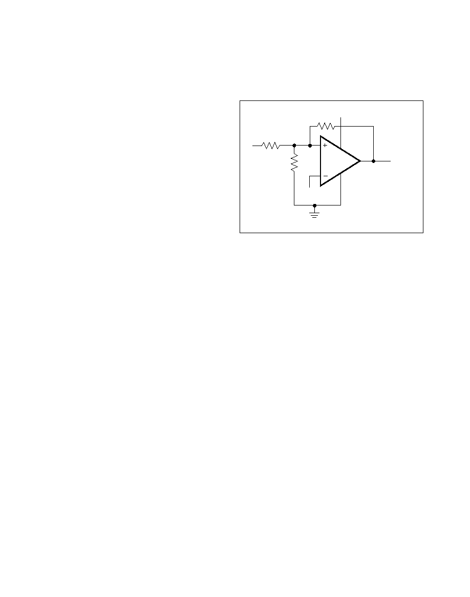
Additional Hysteresis
MAX985/MAX989/MAX993
The MAX985/MAX989/MAX993 have ±3mV internal
hysteresis. Additional hysteresis can be generated with
three resistors using positive feedback (Figure 1).
Unfortunately, this method also slows hysteresis
response time. Use the following procedure to calcu-
late resistor values for the MAX985/MAX989/MAX993.
1) Select R3. Leakage current at IN is under 10nA, so
the current through R3 should be at least 1A to
minimize errors caused by leakage current. The cur-
rent through R3 at the trip point is (VREF - VOUT) /
R3. Considering the two possible output states in
solving for R3 yields two formulas: R3 = VREF / 1A
or R3 = (VREF - VCC) / 1A. Use the smaller of the
two resulting resistor values. For example, if VREF =
1.2V and VCC = 5V, then the two R3 resistor values
are 1.2M
and 3.8M. Choose a 1.2M standard
value for R3.
2) Choose the hysteresis band required (VHB). For this
example, choose 50mV.
3) Calculate R1 according to the following equation:
R1 = R3 x (VHB / VCC)
For this example, insert the values R1 = 1.2M
x
(50mV / 5V) = 12k
.
4) Choose the trip point for VIN rising (VTHR; VTHF is
the trip point for VIN falling). This is the threshold
voltage at which the comparator switches its output
from low to high as VIN rises above the trip point. For
this example, choose 3V.
VCC
MAX985
MAX989
MAX993
OUT
R3
R1
R2
VREF
VEE
VIN
VCC
Figure 1. Additional Hysteresis (MAX985/MAX989/MAX993)
相关PDF资料 |
PDF描述 |
|---|---|
| VE-JNY-MY-F1 | CONVERTER MOD DC/DC 3.3V 33W |
| VE-JNY-MX-F4 | CONVERTER MOD DC/DC 3.3V 49.5W |
| VE-JNY-MX-F2 | CONVERTER MOD DC/DC 3.3V 49.5W |
| VI-B60-MX-F3 | CONVERTER MOD DC/DC 5V 75W |
| VI-B60-MX-F2 | CONVERTER MOD DC/DC 5V 75W |
相关代理商/技术参数 |
参数描述 |
|---|---|
| MAX9860ETG+ | 功能描述:接口—CODEC 16-Bit Mono Audio Voice CODEC RoHS:否 制造商:Texas Instruments 类型: 分辨率: 转换速率:48 kSPs 接口类型:I2C ADC 数量:2 DAC 数量:4 工作电源电压:1.8 V, 2.1 V, 2.3 V to 5.5 V 最大工作温度:+ 85 C 安装风格:SMD/SMT 封装 / 箱体:DSBGA-81 封装:Reel |
| MAX9860ETG+ | 制造商:Maxim Integrated Products 功能描述:AUDIO CODEC 16BIT MONO 24TQFN |
| MAX9860ETG+ | 制造商:Maxim Integrated Products 功能描述:IC AUDIO CODEC 16BIT 48KHZ 制造商:Maxim Integrated Products 功能描述:IC, AUDIO CODEC, 16BIT, 48KHZ, TQFN-24 |
| MAX9860ETG+T | 功能描述:接口—CODEC 16-Bit Mono Audio Voice CODEC RoHS:否 制造商:Texas Instruments 类型: 分辨率: 转换速率:48 kSPs 接口类型:I2C ADC 数量:2 DAC 数量:4 工作电源电压:1.8 V, 2.1 V, 2.3 V to 5.5 V 最大工作温度:+ 85 C 安装风格:SMD/SMT 封装 / 箱体:DSBGA-81 封装:Reel |
| MAX9860EVKIT+ | 功能描述:音频 IC 开发工具 MAX9860 Eval Kit RoHS:否 制造商:Texas Instruments 产品:Evaluation Kits 类型:Audio Amplifiers 工具用于评估:TAS5614L 工作电源电压:12 V to 38 V |
发布紧急采购,3分钟左右您将得到回复。