- 您现在的位置:买卖IC网 > PDF目录5819 > MAX9939AUB+ (Maxim Integrated Products)IC AMP PGA SPI VOS I/O 10MSOP PDF资料下载
参数资料
| 型号: | MAX9939AUB+ |
| 厂商: | Maxim Integrated Products |
| 文件页数: | 13/15页 |
| 文件大小: | 0K |
| 描述: | IC AMP PGA SPI VOS I/O 10MSOP |
| 产品培训模块: | Lead (SnPb) Finish for COTS Obsolescence Mitigation Program |
| 标准包装: | 50 |
| 放大器类型: | 可编程增益 |
| 电路数: | 2 |
| 输出类型: | 差分 |
| 转换速率: | 9 V/µs |
| 增益带宽积: | 2.15MHz |
| 电流 - 输入偏压: | 1pA |
| 电压 - 输入偏移: | 1500µV |
| 电流 - 电源: | 3.4mA |
| 电流 - 输出 / 通道: | 70mA |
| 电压 - 电源,单路/双路(±): | 2.9 V ~ 5.5 V |
| 工作温度: | -40°C ~ 125°C |
| 安装类型: | 表面贴装 |
| 封装/外壳: | 10-TFSOP,10-MSOP(0.118",3.00mm 宽) |
| 供应商设备封装: | 10-µMAX |
| 包装: | 管件 |
| 产品目录页面: | 1392 (CN2011-ZH PDF) |
Detailed Description
The MAX9939 is a general-purpose PGA with input off-
set trim capability. Its gain and input offset voltage
(VOS) are SPI programmable. The device also includes
an uncommitted output operational amplifier that can
be used as either a high-order active filter or to provide
a differential output. The device can be put into shut-
down through SPI.
The gain of the amplifier is programmable between
0.2V/V and 157V/V. The input offset is programmable
between ±17mV and can be used to regain output
dynamic range in high gain settings. An input offset-volt-
age measurement mode enables input offset voltage to
be calibrated out in firmware to obtain excellent DC
accuracy.
The main amplifier accepts a differential input and pro-
vides a single-ended output. The relationship between
the differential input and singled-ended output is given
by the representative equation:
VOUTA = VCC/2 - Gain x (VINA+ - VINA-) + Gain x VOS
Architecture
The MAX9939 features three internal amplifiers as
shown in the
Functional Diagram. The first amplifier
(amplifier LVL) is configured as a differential amplifier
for differential to single-ended conversion with an input
offset-voltage trim network. It has extremely high
Typical Operating Characteristics (continued)
(VCC = 5V, VGND = 0V, VIN+ = VIN- = 0V, Gain = 10V/V, ROUTA = ROUTB = 1k to VCC/2, TA = +25°C, unless otherwise noted.)
Pin Description
PIN
NAME
FUNCTION
1
SCLK
Serial-Clock Input
2
DIN
Serial-Data Input. Data is clocked into the serial interface on the rising edge of SCLK.
3
GND
Ground
4
INA-
PGA Inverting Input
5
INA+
PGA Noninverting Input
6
OUTB
Buffer Output
7
INB
Buffer Input
8
OUTA
PGA Output
9VCC
Power Supply. Bypass to GND with 0.1F and 1F capacitors.
10
CS
Active-Low Chip-Select Input. Drive
CS low to enable the serial interface. Drive CS high to disable the serial interface.
MAX9939
SPI Programmable-Gain Amplifier
with Input VOS Trim and Output Op Amp
7
Maxim Integrated
200
s/div
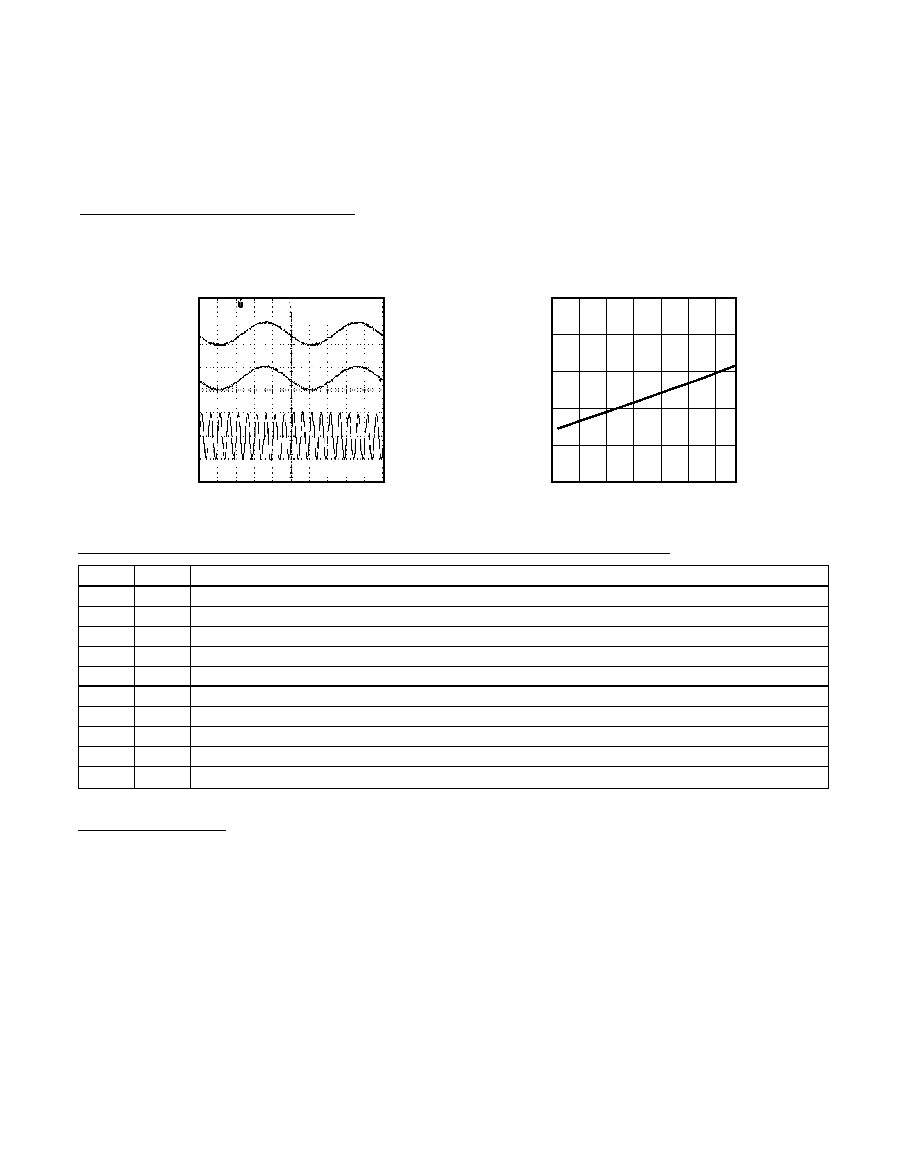
COMMON-MODE REJECTION RESPONSE
INA+
1V/div
INA-
1V/div
MAX9939 toc19
OUTA
2V/div
VCM = 1VP-P, 1kHz
VDM = 25mVP-P, 10kHz
GAIN = 157V/V
SHUTDOWN CURRENT vs. SUPPLY VOLTAGE
MAX9939
toc20
VOLTAGE (V)
SHUTDOWN
CURRENT
(
A)
3.6
4.0
16
20
8
4
12
0
2.8
3.2
4.8
5.2
4.4
相关PDF资料 |
PDF描述 |
|---|---|
| 77311-101-26LF | BERGSTIK |
| 170M3523 | FUSE 630A 690V 1GN/50 |
| 73085-6 | TERMINAL JACK MALE 10-32 BLUE |
| MAX4472EUD+ | IC OP AMP QUAD R-R 9KHZ 14-TSSOP |
| BK/C519-7-R | FUSE 7.00A 125V T-LAG GLASS C519 |
相关代理商/技术参数 |
参数描述 |
|---|---|
| MAX9939AUB/GG8 | 制造商:Maxim Integrated Products 功能描述:SPI-PROGRAMMABLE GAIN AMPLIFIER (PG - Rail/Tube |
| MAX9939AUB/GH9 | 制造商:Maxim Integrated Products 功能描述:SPI-PROGRAMMABLE GAIN AMPLIFIER - Rail/Tube |
| MAX9939AUB/V+ | 功能描述:特殊用途放大器 SPI-Programmable Gain Amplifier (PGA) with Input VOS Trim and Output Op Amp RoHS:否 制造商:Texas Instruments 通道数量:Single 共模抑制比(最小值): 输入补偿电压: 工作电源电压:3 V to 5.5 V 电源电流:5 mA 最大功率耗散: 最大工作温度:+ 70 C 最小工作温度:- 40 C 安装风格:SMD/SMT 封装 / 箱体:QFN-20 封装:Reel |
| MAX9939AUB/V+T | 功能描述:特殊用途放大器 SPI-Programmable Gain Amplifier (PGA) with Input VOS Trim and Output Op Amp RoHS:否 制造商:Texas Instruments 通道数量:Single 共模抑制比(最小值): 输入补偿电压: 工作电源电压:3 V to 5.5 V 电源电流:5 mA 最大功率耗散: 最大工作温度:+ 70 C 最小工作温度:- 40 C 安装风格:SMD/SMT 封装 / 箱体:QFN-20 封装:Reel |
| MAX9939AUB+ | 功能描述:电流灵敏放大器 SPI-Programmable Gain Amplifier RoHS:否 制造商:Texas Instruments 通道数量: 共模抑制比(最小值):110 dB 输入补偿电压:80 uV 电源电压-最大:5.5 V 电源电压-最小:2.7 V 电源电流:350 uA 最大工作温度:+ 125 C 最小工作温度:- 40 C 安装风格:SMD/SMT 封装 / 箱体:VQFN-16 封装:Reel |
发布紧急采购,3分钟左右您将得到回复。