- 您现在的位置:买卖IC网 > PDF目录2159 > MAX9943AUA+T (Maxim Integrated Products)IC OPAMP PREC LP/HV SGL 8-MSOP PDF资料下载
参数资料
| 型号: | MAX9943AUA+T |
| 厂商: | Maxim Integrated Products |
| 文件页数: | 8/15页 |
| 文件大小: | 0K |
| 描述: | IC OPAMP PREC LP/HV SGL 8-MSOP |
| 产品培训模块: | Lead (SnPb) Finish for COTS Obsolescence Mitigation Program |
| 标准包装: | 2,500 |
| 放大器类型: | 通用 |
| 电路数: | 1 |
| 输出类型: | 满摆幅 |
| 转换速率: | 0.35 V/µs |
| 增益带宽积: | 2.4MHz |
| 电流 - 输入偏压: | 4nA |
| 电压 - 输入偏移: | 20µV |
| 电流 - 电源: | 550µA |
| 电流 - 输出 / 通道: | 20mA |
| 电压 - 电源,单路/双路(±): | 6 V ~ 38 V,±3 V ~ 19 V |
| 工作温度: | -40°C ~ 125°C |
| 安装类型: | 表面贴装 |
| 封装/外壳: | 8-TSSOP,8-MSOP(0.118",3.00mm 宽) |
| 供应商设备封装: | 8-uMAX |
| 包装: | 带卷 (TR) |
MAX9943/MAX9944
High-Voltage, Precision, Low-Power Op Amps
2
_______________________________________________________________________________________
ABSOLUTE MAXIMUM RATINGS
Stresses beyond those listed under “Absolute Maximum Ratings” may cause permanent damage to the device. These are stress ratings only, and functional
operation of the device at these or any other conditions beyond those indicated in the operational sections of the specifications is not implied. Exposure to
absolute maximum rating conditions for extended periods may affect device reliability.
Supply Voltage (VCC to VEE) ..................................-0.3V to +40V
All Other Pins (Note 1) .....................(VEE - 0.3V) to (VCC + 0.3V)
OUT Short-Circuit Current Duration
8-Pin μMAX (VCC - VEE ≤ 20V)...............................................3s
8-Pin μMAX (VCC - VEE > 20V) ................................Momentary
6-Pin TDFN (VCC - VEE ≤ 20V) .............................................60s
6-Pin TDFN (VCC - VEE > 20V)...............................................2s
8-Pin SO (VCC - VEE ≤ 20V) .................................................60s
8-Pin SO (VCC - VEE > 20V)...................................................2s
8-Pin TDFN (VCC - VEE ≤ 20V) .............................................60s
8-Pin TDFN (VCC - VEE > 20V)...............................................2s
Continuous Input Current (Any Pins) ................................±20mA
Thermal Limits (Note 2)
Multiple Layer PCB
Continuous Power Dissipation (TA = +70°C)
8-Pin μMAX (derate 4.8mW/°C above +70°C) ...........387.8mW
6-Pin TDFN-EP (derate 23.8mW/°C above +70°C) ..1904.8mW
8-Pin SO (derate 7.6mW/°C above +70°C)...................606.1W
8-Pin TDFN-EP (derate 24.4mW/°C above +70°C) ..1951.2mW
Operating Temperature Range .........................-40°C to +125°C
Junction Temperature ......................................................+150°C
Lead Temperature (soldering, 10s) .................................+300°C
Soldering Temperature (reflow) .......................................+260°C
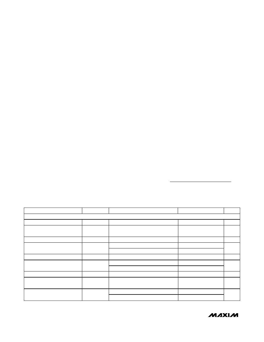
PARAMETER
SYMBOL
CONDITIONS
MIN
TYP
MAX
UNITS
DC CHARACTERISTICS
Operating Supply Voltage Range
VSUPPLY
Guaranteed by PSRR test
±3
±19
V
Quiescent Supply Current per
Amplifier
ICC
550
950
μA
Power-Supply Rejection Ratio
PSRR
VS =
±3V to ±19V
105
130
dB
TA = +25
°C
20
100
Input Offset Voltage
VOS
TA = -40
°C to +125°C
240
μV
Input Offset Voltage Drift
TCVOS
0.4
μV/
°C
VEE + 0.3V
≤ VCM ≤ VCC - 1.8V
4
20
Input Bias Current
IBIAS
VEE
≤ VCM ≤ VCC - 1.8V
90
nA
Input Offset Current
IOS
VEE
≤ VCM ≤ VCC - 1.8V
1
10
nA
Input Voltage Range
VIN+ , VIN-
Guaranteed by CMRR test,
TA = -40
°C to +125°C
VEE
VCC -
1.8
V
VEE + 0.3V
≤ VCM ≤ VCC - 1.8V
105
125
Common-Mode Rejection Ratio
CMRR
VEE
≤ VCM ≤ VCC - 1.8V
105
dB
ELECTRICAL CHARACTERISTICS
(VCC = 15V, VEE = -15V, VCM = 0V, RL = 10kΩ to GND, VGND = 0V, TA = -40°C to +125°C. Typical values are at TA = +25°C, unless
otherwise noted.) (Note 3)
Note 1: Operation is limited by thermal limits.
Note 2: Package thermal resistances were obtained using the method described in JEDEC specification JESD51-7, using a four-
layer board. For detailed information on package thermal considerations, refer to www.maxim-ic.com/thermal-tutorial.
8 μMAX
Junction-to-Ambient Thermal Resistance (
θJA)......206.3°C/W
Junction-to-Ambient Case Resistance (
θJC) ...............42°C/W
6 TDFN-EP
Junction-to-Ambient Thermal Resistance (
θJA)...........42°C/W
Junction-to-Ambient Case Resistance (
θJC) .................9°C/W
8 SO
Junction-to-Ambient Thermal Resistance (
θJA).........132°C/W
Junction-to-Ambient Case Resistance (
θJC) ...............38°C/W
8 TDFN-EP
Junction-to-Ambient Thermal Resistance (
θJA)...........41°C/W
Junction-to-Ambient Case Resistance (
θJC) .................8°C/W
PACKAGE THERMAL CHARACTERISTICS (Note 2)
相关PDF资料 |
PDF描述 |
|---|---|
| MAX9945AUA+T | IC OPAMP MOS-INPUT LP/LN 8-MSOP |
| MC33077P | IC OPAMP DUAL LOW NOISE 8DIP |
| MC33079PG | IC OPAMP QUAD LOW NOISE 14DIP |
| MC33178DMR2G | IC OPAMP DUAL LOW PWR/NS MICRO8 |
| MC33201VDG | IC OPAMP SGL R-R LOW VOLT 8SOIC |
相关代理商/技术参数 |
参数描述 |
|---|---|
| MAX9943EVKIT+ | 功能描述:放大器 IC 开发工具 MAX9943 Eval Kit RoHS:否 制造商:International Rectifier 产品:Demonstration Boards 类型:Power Amplifiers 工具用于评估:IR4302 工作电源电压:13 V to 23 V |
| MAX9944ASA+ | 功能描述:精密放大器 Precision Op Amp RoHS:否 制造商:Maxim Integrated 每芯片的通道数量: 输入补偿电压:0.25 mV at +/- 5 V 输入电压范围(最大值): 安装风格: 封装 / 箱体:SOIC-8 Narrow 封装:Tube |
| MAX9944ASA+T | 功能描述:精密放大器 Precision Op Amp RoHS:否 制造商:Maxim Integrated 每芯片的通道数量: 输入补偿电压:0.25 mV at +/- 5 V 输入电压范围(最大值): 安装风格: 封装 / 箱体:SOIC-8 Narrow 封装:Tube |
| MAX9944ATA+ | 制造商:Maxim Integrated Products 功能描述: |
| MAX9944ATA+T | 功能描述:精密放大器 Precision Op Amp RoHS:否 制造商:Maxim Integrated 每芯片的通道数量: 输入补偿电压:0.25 mV at +/- 5 V 输入电压范围(最大值): 安装风格: 封装 / 箱体:SOIC-8 Narrow 封装:Tube |
发布紧急采购,3分钟左右您将得到回复。