- 您现在的位置:买卖IC网 > PDF目录16897 > MAX9945EVKIT+ (Maxim Integrated Products)EVALUATION KIT FOR MAX9945 PDF资料下载
参数资料
| 型号: | MAX9945EVKIT+ |
| 厂商: | Maxim Integrated Products |
| 文件页数: | 7/14页 |
| 文件大小: | 0K |
| 描述: | EVALUATION KIT FOR MAX9945 |
| 产品培训模块: | Lead (SnPb) Finish for COTS Obsolescence Mitigation Program |
| 标准包装: | 1 |
| 每 IC 通道数: | 1 - 单 |
| 放大器类型: | 通用 |
| 输出类型: | 单端,满摆幅 |
| 转换速率: | 2.2 V/µs |
| 电流 - 输出 / 通道: | 25mA |
| 工作温度: | -40°C ~ 125°C |
| 电流供应(主 IC): | 400µA |
| 电压 - 电源,单路/双路(±): | 4.75 V ~ 38 V,±2.4 V ~ 19 V |
| 板类型: | 完全填充 |
| 已供物品: | 板 |
| 已用 IC / 零件: | MAX9945 |
MAX9945
38V, Low-Noise, MOS-Input,
Low-Power Op Amp
2
_______________________________________________________________________________________
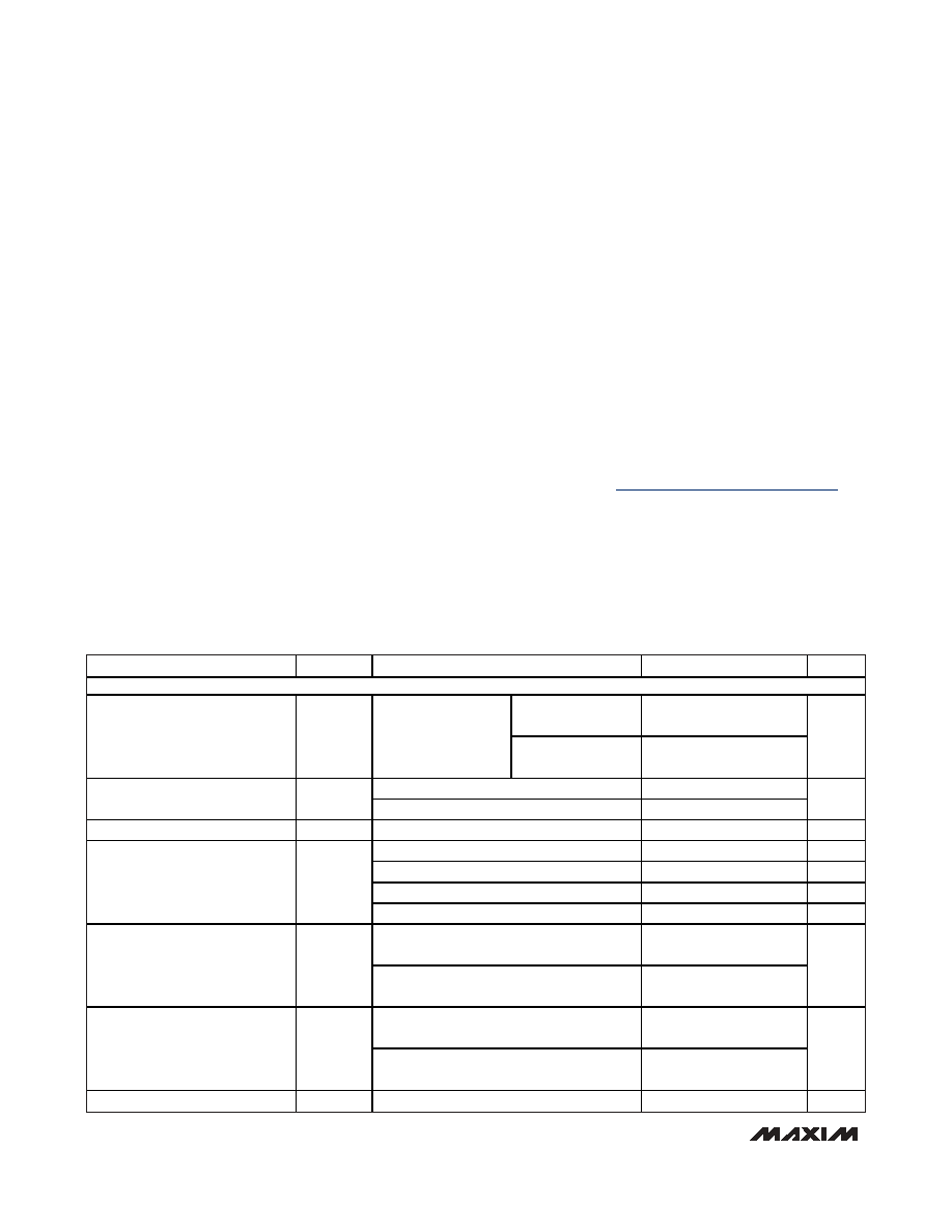
ABSOLUTE MAXIMUM RATINGS
ELECTRICAL CHARACTERISTICS
(VCC = +15V, VEE = -15V, VIN+ = VIN- = VGND = 0V, ROUT = 100kΩ to GND, TA = -40°C to +125°C, typical values are at TA = +25°C,
unless otherwise noted.) (Note 2)
Stresses beyond those listed under “Absolute Maximum Ratings” may cause permanent damage to the device. These are stress ratings only, and functional
operation of the device at these or any other conditions beyond those indicated in the operational sections of the specifications is not implied. Exposure to
absolute maximum rating conditions for extended periods may affect device reliability.
Supply Voltage (VCC to VEE) ..................................-0.3V to +40V
IN+, IN-, OUT Voltage......................(VEE - 0.3V) to (VCC + 0.3V)
IN+ to IN- .............................................................................±12V
OUT Short Circuit to Ground Duration....................................10s
Continuous Input Current into Any Pin .............................±20mA
Continuous Power Dissipation (TA = +70°C)
6-Pin TDFN-EP (derate 23.8mW/°C above +70°C)
Multilayer Board ....................................................1904.8mW
8-Pin MAX (derate 4.8mW/°C above +70°C)
Multilayer Board ......................................................387.8mW
Operating Temperature Range .........................-40°C to +125°C
Junction Temperature ......................................................+150°C
Storage Temperature Range .............................-65°C to +150°C
Lead Temperature (soldering, 10s) .................................+300°C
Soldering Temperature ....................................................+260°C
PARAMETER
SYMBOL
CONDITIONS
MIN
TYP
MAX
UNITS
DC ELECTRICAL CHARACTERISTICS
TA = +25°C
VEE
VCC -
1.2
Input Voltage Range
VIN+, VIN-
Guaranteed by
CMRR
TA = TMIN to TMAX
VEE
VCC -
1.4
V
TA = +25°C
±0.6
±5
Input Offset Voltage
VOS
TA = TMIN to TMAX
±8
mV
Input Offset Voltage Drift
VOS - TC
2
V/°C
-40°C
≤ TA ≤ +25°C
50
150
fA
-40°C
≤ TA ≤ +70°C
12
pA
-40°C
≤ TA ≤ +85°C
55
pA
Input Bias Current (Note 3)
IB
-40°C
≤ TA ≤ +125°C
1.9
nA
VCM = VEE to VCC - 1.2V,
TA = +25°C
78
94
Common-Mode Rejection Ratio
CMRR
VCM = VEE to VCC - 1.4V,
TA = TMIN to TMAX
78
94
dB
VEE + 0.3V
≤ VOUT ≤ VCC - 0.3V,
ROUT = 100k
Ω to GND
110
130
Open-Loop Gain
AOL
VEE + 0.75V
≤ VOUT ≤ VCC - 0.75V,
ROUT = 10k
Ω to GND
110
130
dB
Output Short-Circuit Current
ISC
25
mA
Note 1: Package thermal resistances were obtained using the method described in JEDEC specification JESD51-7, using a four-
layer board. For detailed information on package thermal considerations, refer to www.maxim-ic.com/thermal-tutorial.
PACKAGE THERMAL CHARACTERISTICS (Note 1)
TDFN-EP
Junction-to-Ambient Thermal Resistance (
θJA) ............42°C/W
Junction-to-Case Thermal Resistance (
θJC) ...................9°C/W
MAX
Junction-to-Ambient Thermal Resistance (
θJA) .......206.3°C/W
Junction-to-Case Thermal Resistance
θJC ...................42°C/W
相关PDF资料 |
PDF描述 |
|---|---|
| 301A022-25/86-0 | BOOT MOLDED |
| IDSD-04-S-06.00-ST8 | CABLE ASSEM 8POS |
| EEC28DREH-S93 | CONN EDGECARD 56POS .100 EYELET |
| LM4040AEX3-3.0+T | IC VREF SHUNT PREC 3V SC-70-3 |
| ECM18DTAN-S189 | CONN EDGECARD 36POS R/A .156 SLD |
相关代理商/技术参数 |
参数描述 |
|---|---|
| MAX9945EVKIT+ | 功能描述:放大器 IC 开发工具 38V MOS-Input Op Amp RoHS:否 制造商:International Rectifier 产品:Demonstration Boards 类型:Power Amplifiers 工具用于评估:IR4302 工作电源电压:13 V to 23 V |
| MAX9947ETE+ | 功能描述:射频收发器 AISG Interface RoHS:否 制造商:Atmel 频率范围:2322 MHz to 2527 MHz 最大数据速率:2000 Kbps 调制格式:OQPSK 输出功率:4 dBm 类型: 工作电源电压:1.8 V to 3.6 V 最大工作温度:+ 85 C 接口类型:SPI 封装 / 箱体:QFN-32 封装:Tray |
| MAX9947ETE+T | 功能描述:射频收发器 AISG Interface RoHS:否 制造商:Atmel 频率范围:2322 MHz to 2527 MHz 最大数据速率:2000 Kbps 调制格式:OQPSK 输出功率:4 dBm 类型: 工作电源电压:1.8 V to 3.6 V 最大工作温度:+ 85 C 接口类型:SPI 封装 / 箱体:QFN-32 封装:Tray |
| MAX9947EVKIT+ | 功能描述:射频开发工具 MAX9947EVKIT+ RoHS:否 制造商:Taiyo Yuden 产品:Wireless Modules 类型:Wireless Audio 工具用于评估:WYSAAVDX7 频率: 工作电源电压:3.4 V to 5.5 V |
| MAX9949DCCB | 制造商:Rochester Electronics LLC 功能描述: 制造商:Maxim Integrated Products 功能描述: |
发布紧急采购,3分钟左右您将得到回复。