- 您现在的位置:买卖IC网 > PDF目录10745 > MAX998EUT+T (Maxim Integrated Products)IC COMP SNGL HI-SPEED LP SOT23-6 PDF资料下载
参数资料
| 型号: | MAX998EUT+T |
| 厂商: | Maxim Integrated Products |
| 文件页数: | 8/11页 |
| 文件大小: | 0K |
| 描述: | IC COMP SNGL HI-SPEED LP SOT23-6 |
| 产品培训模块: | Lead (SnPb) Finish for COTS Obsolescence Mitigation Program |
| 标准包装: | 1 |
| 类型: | 通用 |
| 元件数: | 1 |
| 输出类型: | CMOS,满摆幅,TTL |
| 电压 - 电源,单路/双路(±): | 2.7 V ~ 5.5 V |
| 电压 - 输入偏移(最小值): | 2mV @ 5V |
| 电流 - 输入偏压(最小值): | 0.075µA @ 5.5V |
| 电流 - 静态(最大值): | 650µA |
| CMRR, PSRR(标准): | 95dB CMRR,100dB PSRR |
| 传输延迟(最大): | 28ns |
| 磁滞: | 5mV |
| 工作温度: | -40°C ~ 85°C |
| 封装/外壳: | SOT-23-6 |
| 安装类型: | 表面贴装 |
| 包装: | 标准包装 |
| 产品目录页面: | 1387 (CN2011-ZH PDF) |
| 其它名称: | MAX998EUT+TDKR |
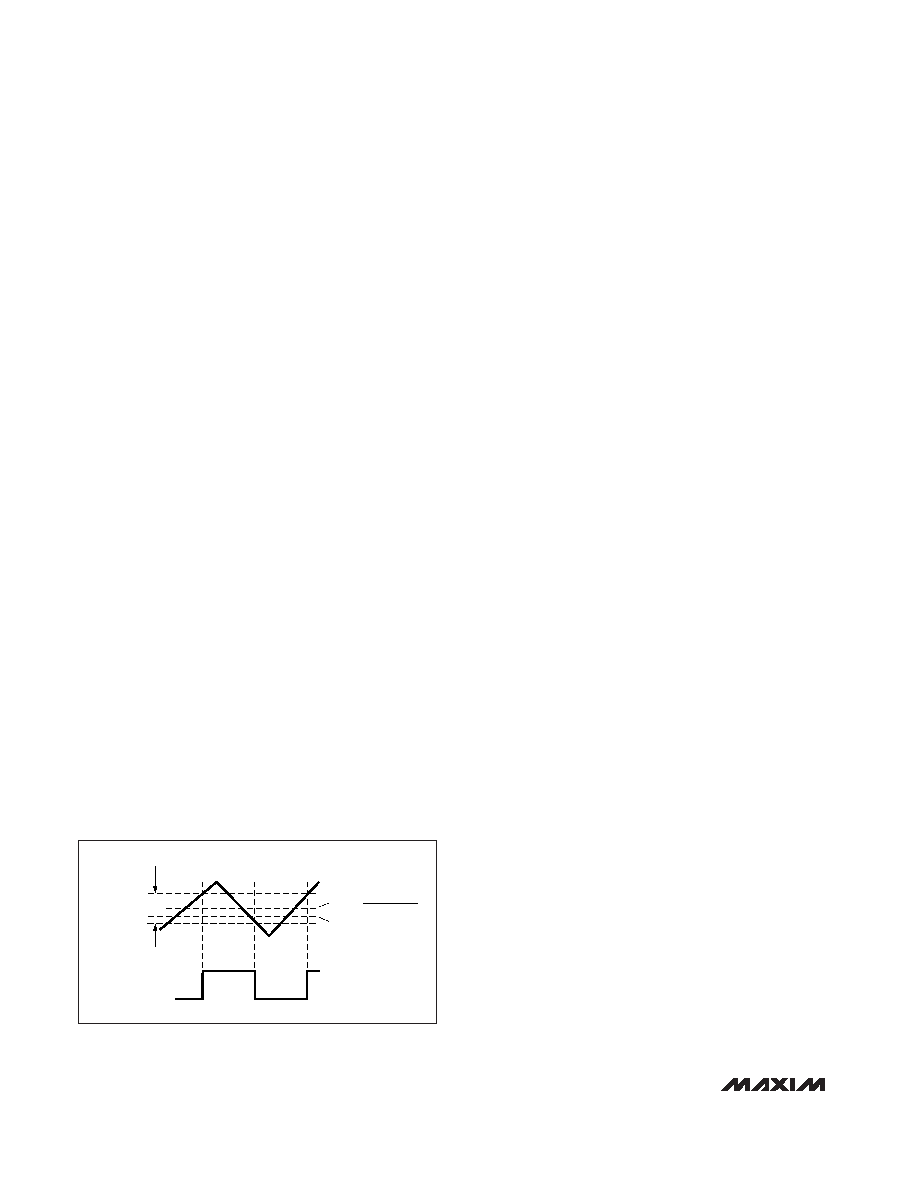
Hysteresis
High-speed comparators can oscillate in the linear
operating region because of noise or undesired para-
sitic feedback. This tends to occur when the voltage on
one input is equal to or very close to the voltage on the
other input. The MAX976/MAX978/MAX998 have inter-
nal hysteresis to counter parasitic effects and noise.
The hysteresis in a comparator creates two trip points:
one for the rising input voltage and one for the falling
input voltage (Figure 1). The difference between the trip
points is the hysteresis. When the comparator input
voltages are equal, the hysteresis effectively causes
one comparator input voltage to move quickly past the
other, taking the input out of the region where oscilla-
tion occurs.
Figure 1 illustrates the case where IN- has a fixed volt-
age applied and IN+ is varied. If the inputs were
reversed, the figure would be the same, except with an
inverted output.
Input-Stage Circuitry
The MAX976/MAX978/MAX998 input common-mode
voltage range is from -0.2V to (VCC - 1.2V). The voltage
range for each comparator input extends to both VCC
and GND. The output remains in the correct logic state
while one or both of the inputs are within the common-
mode range. If both input levels are out of the common-
mode range, input-stage current saturation occurs, and
the output becomes unpredictable.
Shutdown Mode
The MAX998 features a low-power shutdown mode,
which is activated by forcing SHDN low. Shutdown
mode reduces the supply current to 1nA (typical), dis-
ables the comparator, and places the output in a high-
impedance state. Drive SHDN high to enable the
comparator. Do not leave SHDN unconnected. Since it
is a high-impedance input, leaving SHDN unconnected
could result in indeterminate logic levels, adversely
affecting comparator operation. Likewise, do not three-
state SHDN. Due to the output leakage currents of
three-state devices and the small internal current for
SHDN, three-stating this pin could also result in indeter-
minate logic levels.
The maximum input voltage for SHDN is 6V, referred to
GND, and is not limited by VCC. This allows the use of
5V logic to drive SHDN while VCC operates at a lower
voltage, such as 3V. The logic threshold limits for
SHDN are proportional to VCC (see Electrical
Characteristics).
_____________Applications Information
Circuit Layout and Bypassing
The MAX976/MAX978/MAX998 have a high-gain band-
width and require careful board layout. We recommend
the following design guidelines:
1) Use a printed circuit board with an unbroken, low-
inductance ground plane. Surface-mount compo-
nents are recommended.
2) Place a decoupling capacitor (a 0.1F ceramic
capacitor is a good choice) between VCC and
ground as close to the pins as possible.
3) Keep lead lengths short on the inputs and outputs
to avoid unwanted parasitic feedback around the
comparators.
4) Solder the devices directly to the printed circuit
board instead of using a socket.
5) Minimize input impedance.
6) For slowly varying inputs, use a small capacitor
(~1000pF) across the inputs to improve stability.
Additional Hysteresis
Generate additional hysteresis with three resistors
using positive feedback, as shown in Figure 2. This
positive feedback method slows the hysteresis
response time. Calculate resistor values as follows:
1) Select R3. The leakage current of IN+ is typically
75nA, so the current through R3 should be at least
1.0A to minimize errors caused by leakage current.
The current through R3 at the trip point is (VREF -
VOUT) / R3. Consider the two possible output states
when solving for R3. The two formulas are:
R3 = VREF / 1.0A
or
R3 = (VCC - VREF) / 1.0A
Use the smaller of the two resulting resistor values.
For example, if VREF = 1.2V and VCC = 5.0V, the two
resistor values are 1.2M
Ω and 3.8MΩ. Choose a
standard value for R3 of 1.2M
Ω.
MAX976/MAX978/MAX998
Single/Dual/Quad, SOT23, Single-Supply,
High-Speed, Low-Power Comparators
6
_______________________________________________________________________________________
VOL
VOH
VIN- = 0
VOS =
VTRIP+ + VTRIP-
2
COMPARATOR
OUTPUT
VTRIP+
VIN+
VHYST
VTRIP-
Figure 1. Input and Output Waveforms, Noninverting Input
Varied
相关PDF资料 |
PDF描述 |
|---|---|
| AD73360ASUZ-REEL | IC ANALOG FRONT END 6CH 44-TQFP |
| AD73360LARZ-REEL7 | IC PROCESSOR FRONTEND 6CH 28SOIC |
| MAX965EUA+ | IC COMPARATOR R-R 8-UMAX |
| MAX966ESA+ | IC COMPARATOR R-R 8-SOIC |
| VE-JN4-MY-F1 | CONVERTER MOD DC/DC 48V 50W |
相关代理商/技术参数 |
参数描述 |
|---|---|
| MAX9990ETP | 功能描述:射频放大器 RoHS:否 制造商:Skyworks Solutions, Inc. 类型:Low Noise Amplifier 工作频率:2.3 GHz to 2.8 GHz P1dB:18.5 dBm 输出截获点:37.5 dBm 功率增益类型:32 dB 噪声系数:0.85 dB 工作电源电压:5 V 电源电流:125 mA 测试频率:2.6 GHz 最大工作温度:+ 85 C 安装风格:SMD/SMT 封装 / 箱体:QFN-16 封装:Reel |
| MAX9990ETP+ | 功能描述:射频放大器 14dBm to 20dBm LO Buffer RoHS:否 制造商:Skyworks Solutions, Inc. 类型:Low Noise Amplifier 工作频率:2.3 GHz to 2.8 GHz P1dB:18.5 dBm 输出截获点:37.5 dBm 功率增益类型:32 dB 噪声系数:0.85 dB 工作电源电压:5 V 电源电流:125 mA 测试频率:2.6 GHz 最大工作温度:+ 85 C 安装风格:SMD/SMT 封装 / 箱体:QFN-16 封装:Reel |
| MAX9990ETP+T | 功能描述:射频放大器 14dBm to 20dBm LO Buffer RoHS:否 制造商:Skyworks Solutions, Inc. 类型:Low Noise Amplifier 工作频率:2.3 GHz to 2.8 GHz P1dB:18.5 dBm 输出截获点:37.5 dBm 功率增益类型:32 dB 噪声系数:0.85 dB 工作电源电压:5 V 电源电流:125 mA 测试频率:2.6 GHz 最大工作温度:+ 85 C 安装风格:SMD/SMT 封装 / 箱体:QFN-16 封装:Reel |
| MAX9990ETP-T | 功能描述:射频放大器 RoHS:否 制造商:Skyworks Solutions, Inc. 类型:Low Noise Amplifier 工作频率:2.3 GHz to 2.8 GHz P1dB:18.5 dBm 输出截获点:37.5 dBm 功率增益类型:32 dB 噪声系数:0.85 dB 工作电源电压:5 V 电源电流:125 mA 测试频率:2.6 GHz 最大工作温度:+ 85 C 安装风格:SMD/SMT 封装 / 箱体:QFN-16 封装:Reel |
| MAX9990EVKIT | 功能描述:射频开发工具 RoHS:否 制造商:Taiyo Yuden 产品:Wireless Modules 类型:Wireless Audio 工具用于评估:WYSAAVDX7 频率: 工作电源电压:3.4 V to 5.5 V |
发布紧急采购,3分钟左右您将得到回复。