- 您现在的位置:买卖IC网 > PDF目录80459 > MB89537APMC1 (FUJITSU LTD) MICROCONTROLLER, PQFP64 PDF资料下载
参数资料
| 型号: | MB89537APMC1 |
| 厂商: | FUJITSU LTD |
| 元件分类: | 微控制器/微处理器 |
| 英文描述: | MICROCONTROLLER, PQFP64 |
| 封装: | 10 X 10 MM, 1.70 MM HEIGHT, 0.50 MM PITCH, PLASTIC, LQFP-64 |
| 文件页数: | 3/72页 |
| 文件大小: | 2290K |
| 代理商: | MB89537APMC1 |
第1页第2页当前第3页第4页第5页第6页第7页第8页第9页第10页第11页第12页第13页第14页第15页第16页第17页第18页第19页第20页第21页第22页第23页第24页第25页第26页第27页第28页第29页第30页第31页第32页第33页第34页第35页第36页第37页第38页第39页第40页第41页第42页第43页第44页第45页第46页第47页第48页第49页第50页第51页第52页第53页第54页第55页第56页第57页第58页第59页第60页第61页第62页第63页第64页第65页第66页第67页第68页第69页第70页第71页第72页
MB89530A Series
DS07-12547-7E
11
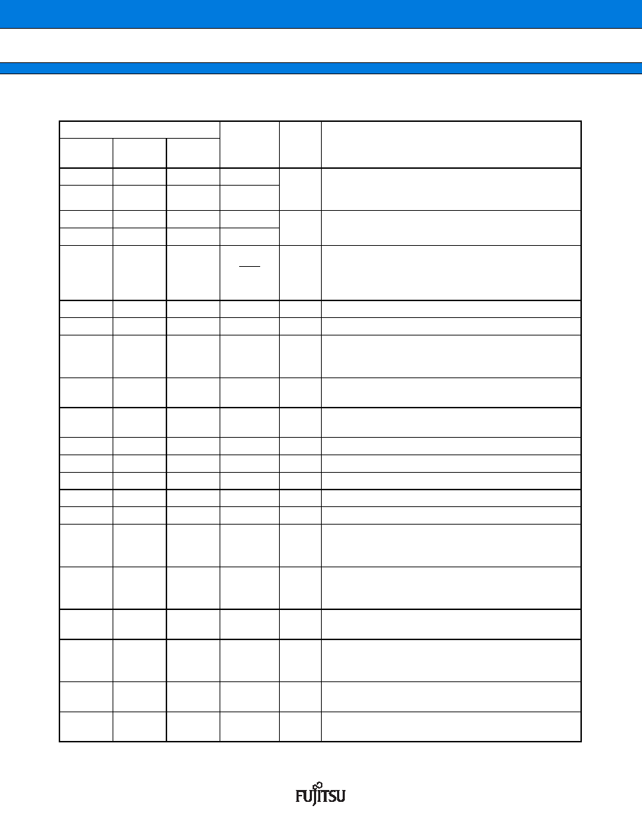
■ PIN DESCRIPTIONS
(Continued)
Pin no.
Pin name
I/O
circuit
type*7
Function
SH-DIP*1
MDIP*2
QFP*3
MQFP*4
LQFP*5
BCC*6
30
23
22
X0
A
Connecting pins to crystal oscillator circuit or other
oscillator circuit. The X0 pin can connect to an external
clock. In that case, X1 is left open.
31
24
23
X1
28
21
20
MOD0
B
Input pins for memory access mode setting.
Connect directly to Vss.
29
22
21
MOD1
27
20
19
RST
C
Reset I/O pin. This pin has pull-up resistance with
CMOS I/O or hysteresis input. At an internal reset
request, an ’L’ signal is output. An ’L’ level input
initializes the internal circuits.
56 to 49
49 to 42
48 to 41
P00 to P07
D
General purpose I/O ports.
48 to 41
41 to 34
40 to 33
P10 to P17
D
General purpose I/O ports.
40
33
32
P20/PWCK
E
General purpose I/O port.Resource I/O pin (hysteresis
input).Hysteresis input. This pin also functions as a
PWC input.
39
32
31
P21/
PPG01
D
General purpose I/O port.This pin also functions as the
PPG01 output.
38
31
30
P22/
PPG02
D
General purpose I/O port.This pin also functions as the
PPG02 output.
37
30
29
P23
D
General purpose I/O port.
36
29
28
P24
D
General purpose I/O port.
35
28
27
P25
D
General purpose I/O port.
34
27
26
P26
D
General purpose I/O port.
33
26
25
P27
D
General purpose I/O port.
58
51
50
P30/
PPG03/
MCO
D
General purpose I/O port.This pin also functions as the
PPG03 output.
59
52
51
P31/SCK1
(UCK1) /
LMCO
E
General purpose I/O port.Resource I/O pin (hysteresis
input).This pin also functions as the UART/SIO clock
input/output pin.
60
53
52
P32/SO1
(UO1)
D
General purpose I/O port.This pin also functions as the
UART/SIO data output pin.
61
54
53
P33/SI1
(UI1)
E
General purpose I/O port.Resource input/output pin
(hysteresis input).This pin also functions as the UART/
SIO serial data input pin.
62
55
54
P34/PTO2
D
General purpose I/O port.This pin also functions as the
PWM timer 2 output pin.
63
56
55
P35/PWC
E
General purpose I/O port.Resource I/O pin (hysteresis
input).This pin also functions as a PWC input.
相关PDF资料 |
PDF描述 |
|---|---|
| MC9S12XF128J0VLH | MICROCONTROLLER, PQFP64 |
| MC9S12XF256J0MLMR | MICROCONTROLLER, PQFP112 |
| MPC8555ECVTAPD | RISC PROCESSOR, PBGA783 |
| MPC8555EVTAKE | RISC PROCESSOR, PBGA783 |
| MPC8572CPXATLB | 32-BIT, 1200 MHz, MICROPROCESSOR, PBGA1023 |
相关代理商/技术参数 |
参数描述 |
|---|---|
| MB89537C | 制造商:FUJITSU 制造商全称:Fujitsu Component Limited. 功能描述:8-bit Original Microcontroller |
| MB89537CP | 制造商:FUJITSU 制造商全称:Fujitsu Component Limited. 功能描述:8-bit Original Microcontroller |
| MB89537CPF | 制造商:FUJITSU 制造商全称:Fujitsu Component Limited. 功能描述:8-bit Original Microcontroller |
| MB89537CPFM | 制造商:FUJITSU 制造商全称:Fujitsu Component Limited. 功能描述:8-bit Original Microcontroller |
| MB89537CPFV | 制造商:FUJITSU 制造商全称:Fujitsu Component Limited. 功能描述:8-bit Original Microcontroller |
发布紧急采购,3分钟左右您将得到回复。