- 您现在的位置:买卖IC网 > PDF目录95879 > MB89538A-64P OTHER CLOCK GENERATOR, PQFP64 PDF资料下载
参数资料
| 型号: | MB89538A-64P |
| 元件分类: | 时钟产生/分配 |
| 英文描述: | OTHER CLOCK GENERATOR, PQFP64 |
| 封装: | 12 X 12 MM, 0.65 MM PITCH, LQFP-64 |
| 文件页数: | 1/5页 |
| 文件大小: | 188K |
| 代理商: | MB89538A-64P |
MB89530A
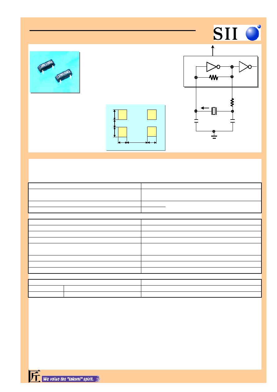
Evaluation of Subsystem Clock Oscillation Circuit
[MB89538A-64P] LQFP(12x12) 0.65mm pitch
Measurement conditions :5.0V , 3.3V
Model
:SP-T2A
Frequency
:Fo=32.768kHz
Frequency tolerance
:dF/Fo= +/-20x10-6
Load capacitance
:CL=6.0pF
Equivalent series resistance :R1=50k ohm max
Max. drive level
:DL=1x10⁻⁶W max
Level of drive
:DL=0.1x10⁻⁶W typ
FEATURES
RECOMMENDED SOLDERING PATTERN
1. Plastic mold package incorporated tubular
type quartz crystal.
2. Suitable for automatic and high density
surface mounting.
3. Excellent shock and heat resistance
4. Real time clocks, Timers,
Portable applications,Clock
source for Micro-Computers
Remark) Ix : current through crystal
MODEL:SP-T2A 6.0pF with MB89538A at 25°C
The above mentioned value is only for your reference. The value is for the arbitrary samples and
does not guarantee the product's characteristics. Please review and check above parameters at customer's end.
Seiko Instruments USA Inc.
Seiko Instruments Inc.
2990,West Lomita Blvd., Torrance, CA 90505, U.S.A
1-8,Nakase,Mihama-ku,Chiba-shi,Chiba 261-8507,Japan
Telephone :+1 310-517-7771 Facsimile :+1 310-517-7792
Facsimile :+81-43-211-8030
Email :crystals@siu-la.com
E-mail :component@sii.co.jp
Seiko Instruments GmbH
Siemensstrasse 9,D-63263 Neu-lsenburg,Germany
Telephone :+49-6102-297-0 Facsimile :+49-6102-297-320
Email :info@seiko-instruments.de
Seiko Instruments Inc.
Phone:+81-43-211-1207(Direct)
-138
Vcc=3.3V
1.5
4.8
Vcc=5.0V
44.9
0.21
Optimal capacity in response to CL
Vcc=3.3V
Negative feedback resistance : Rf ( M ohm )
Built-in
19-Nov-07
Key specifications
Vcc=5.0V
Remarks
Matching Accuracy : df / f ( x10
-6 )
Voltage Fluctuation : +/-df / V ( x10
-6 )
Circuit characteristics ( at 25°C )
2244
Drive Level : DL ( x10
-6W )
Negative resistance : | - RL | ( kohm )
( CL = Cd // Cg + stray capacitance )
Current control resistance : Rd ( k ohm )
Capacitance at drain : Cd ( pF )
Capacitance at gate : Cg ( pF )
470
7
79
470
9
6.1
2.4
0.06
0.05
-127
-139
Variation : df / T ( x10
-6 )
Oscillation allowance : M ( times )
66.9
Voltage of oscillation start : Vstart (V )
Voltage of oscillation stop : Vstop (V )
1.89
1.41
Variation : df / T ( x10
-6 )
Vcc=3.3V
Oscillation start up time : Ts ( sec )
Temperature characteristics of circuit
at +85°C
-127
at 40°C
5 times larger than R1MAX
Judgemental standard of oscillation stability
Vcc=5.0V
Time to reach 90% of output level
1.91
1.43
3344
0.19
Typ.Tp=25°C ( K = -3.5×10
-8 / °C2 )
Control drive level & secure phase margin
Remarks
Frequency offset volume at specified Vdd
Vdd +/-10% ( Standard operating voltage range )
Remarks
Typ.Tp=25°C ( K = -3.5×10
-8 / °C2 )
DL=Ix
2 Re < 1x10⁻⁶W,Re=R1( 1 + Co / CL )2
CL=
CgCd / (Cg+Cd)+Cs
Vss
IC
X0A
X1A
Vcc=2.2V to 5.5V
Ix
32.768kHz
Rd
Cd
Cg
Rf
Unit:mm
1.
3
1.3
4.2
1.
9
1.
9
相关PDF资料 |
PDF描述 |
|---|---|
| MBB100AS6 | 100 A, 600 V, N-CHANNEL IGBT |
| MBB50AS6 | 50 A, 600 V, N-CHANNEL IGBT |
| MBN400C33 | 400 A, 3300 V, N-CHANNEL IGBT |
| MBB75AS6 | 75 A, 600 V, N-CHANNEL IGBT |
| MBM150GS6A | 150 A, 600 V, N-CHANNEL IGBT |
相关代理商/技术参数 |
参数描述 |
|---|---|
| MB89538AC | 制造商:FUJITSU 制造商全称:Fujitsu Component Limited. 功能描述:8-bit Original Microcontroller CMOS, F-2MC-8L MB89530A Series |
| MB89538ACP | 制造商:FUJITSU 制造商全称:Fujitsu Component Limited. 功能描述:8-bit Original Microcontroller CMOS, F-2MC-8L MB89530A Series |
| MB89538ACPF | 制造商:FUJITSU 制造商全称:Fujitsu Component Limited. 功能描述:8-bit Original Microcontroller CMOS, F-2MC-8L MB89530A Series |
| MB89538ACPFM | 制造商:FUJITSU 制造商全称:Fujitsu Component Limited. 功能描述:8-bit Original Microcontroller CMOS, F-2MC-8L MB89530A Series |
| MB89538ACPFV | 制造商:FUJITSU 制造商全称:Fujitsu Component Limited. 功能描述:8-bit Original Microcontroller CMOS, F-2MC-8L MB89530A Series |
发布紧急采购,3分钟左右您将得到回复。