- 您现在的位置:买卖IC网 > PDF目录45188 > MB90671PF 16-BIT, MROM, 16 MHz, MICROCONTROLLER, PQFP80 PDF资料下载
参数资料
| 型号: | MB90671PF |
| 元件分类: | 微控制器/微处理器 |
| 英文描述: | 16-BIT, MROM, 16 MHz, MICROCONTROLLER, PQFP80 |
| 封装: | PLASTIC, QFP-80 |
| 文件页数: | 21/106页 |
| 文件大小: | 1648K |
| 代理商: | MB90671PF |
第1页第2页第3页第4页第5页第6页第7页第8页第9页第10页第11页第12页第13页第14页第15页第16页第17页第18页第19页第20页当前第21页第22页第23页第24页第25页第26页第27页第28页第29页第30页第31页第32页第33页第34页第35页第36页第37页第38页第39页第40页第41页第42页第43页第44页第45页第46页第47页第48页第49页第50页第51页第52页第53页第54页第55页第56页第57页第58页第59页第60页第61页第62页第63页第64页第65页第66页第67页第68页第69页第70页第71页第72页第73页第74页第75页第76页第77页第78页第79页第80页第81页第82页第83页第84页第85页第86页第87页第88页第89页第90页第91页第92页第93页第94页第95页第96页第97页第98页第99页第100页第101页第102页第103页第104页第105页第106页
MB90670/675 Series
21
s HANDLING DEVICES
1.
Make Sure that the Voltage not Exceed the Maximum Rating (to Avoid a Latch-up).
In CMOS ICs, a latch-up phenomenon is caused when an voltage exceeding VCC or an voltage below VSS is
applied to input or output pins or a voltage exceeding the rating is applied across VCC and VSS.
When a latch-up is caused, the power supply current may be dramatically increased causing resultant thermal
break-down of devices. To avoid the latch-up, make sure that the voltage not exceed the maximum rating.
In turning on/turning off the analog power supply, make sure the analog power voltage (AVCC, AVRH) and analog
input voltages not exceed the digital voltage (VCC).
2.
Connection of Unused Pins
Leaving unused pins open may result in abnormal operations. Clamp the pin level by connecting it to a pull-up
or a pull-down resistor.
3.
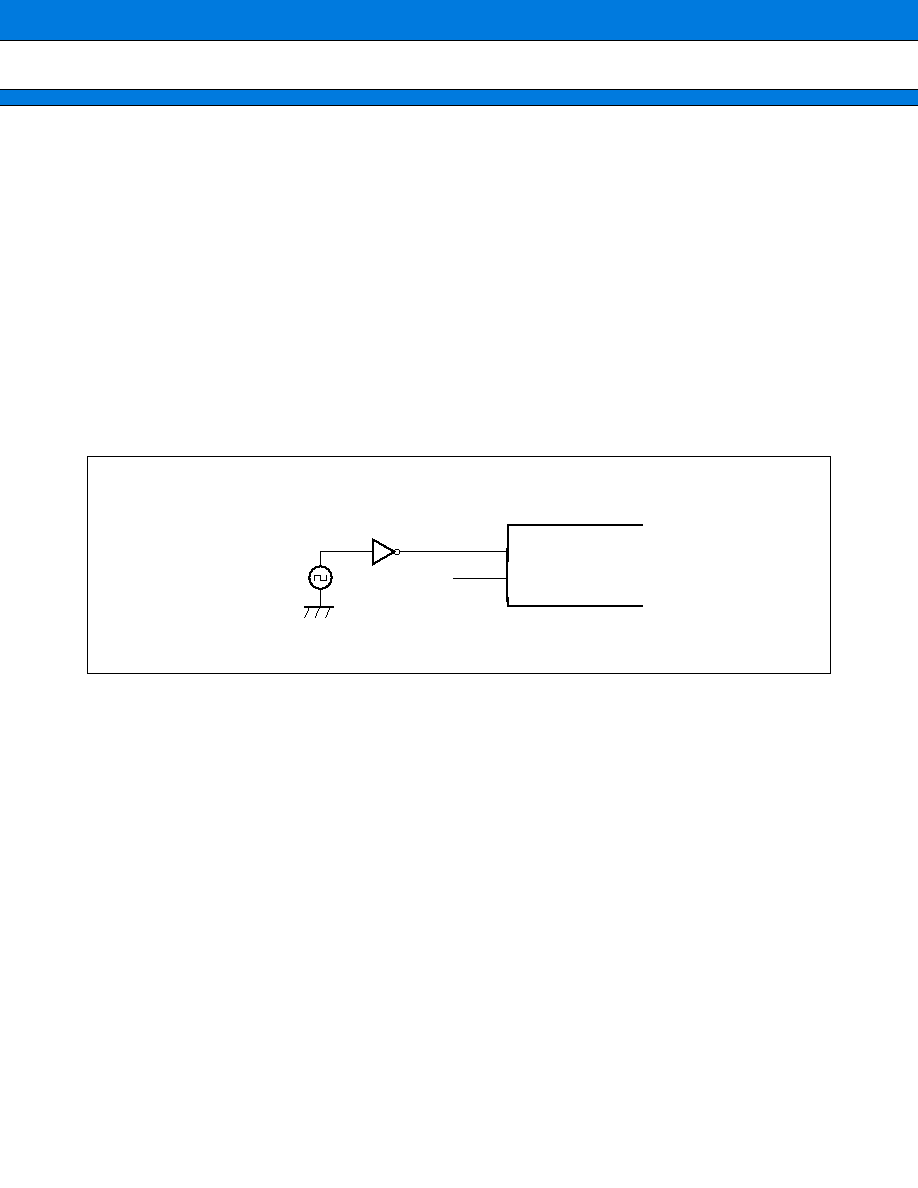
Notes on Using External Clock
In using the external clock, drive X0 pin only and leave X1 pin unconnected.
4.
Power Supply Pins
In products with multiple VCC or VSS pins, the pins of a same potential are internally connected in the device to
avoid abnormal operations including latch-up. However, connect the pins external power and ground lines to
lower the electro-magnetic emission level and abnormal operation of strobe signals caused by the rise in the
ground level, and to conform to the total current rating.
Make sure to connect VCC and VSS pins via lowest impedance to power lines.
It is recommended to provide a bypass capacitor of around 0.1
F between VCC and VSS pin near the device.
5.
Crystal Oscillator Circuit
Noises around X0 or X1 pins may be possible causes of abnormal operations. Make sure to provide bypass
capacitors via shortest distance from X0, X1 pins, crystal oscillator (or ceramic resonator) and ground lines, and
make sure, to the utmost effort, that lines of oscillation circuit not cross the lines of other circuits.
It is highly recommended to provide a printed circuit board art work surrounding X0 and X1 pins with an grand
area for stabilizing the operation.
6.
Turning-on Sequence of Power Supply to A/D Converter and Analog Inputs
Make sure to turn on the A/D converter power supply (AVCC, AVRH, AVRL) and analog inputs (AN0 to AN7) after
turning-on the digital power supply (VCC).
Turn-off the digital power after turning off the A/D converter supply and analog inputs. In this case, make sure
that the voltage not exceed AVRH or AVCC (turning on/off the analog and digital power supplies simultaneously
is acceptable).
Using external clock
X0
X1
Open
MB90670/675 series
相关PDF资料 |
PDF描述 |
|---|---|
| MB90P678PF | 16-BIT, OTPROM, 16 MHz, MICROCONTROLLER, PQFP100 |
| MB90T673PFV | 16-BIT, 16 MHz, MICROCONTROLLER, PQFP80 |
| MB90P673PFV | 16-BIT, OTPROM, 16 MHz, MICROCONTROLLER, PQFP80 |
| MB90P673PF | 16-BIT, OTPROM, 16 MHz, MICROCONTROLLER, PQFP80 |
| MB90802SPF-G | 16-BIT, MROM, 25 MHz, MICROCONTROLLER, PQFP100 |
相关代理商/技术参数 |
参数描述 |
|---|---|
| MB90671PFV | 制造商:FUJITSU 制造商全称:Fujitsu Component Limited. 功能描述:16-Bit Proprietary Microcontroller |
| MB90672 | 制造商:FUJITSU 制造商全称:Fujitsu Component Limited. 功能描述:16-Bit Proprietary Microcontroller |
| MB90672PF | 制造商:FUJITSU 制造商全称:Fujitsu Component Limited. 功能描述:16-Bit Proprietary Microcontroller |
| MB90672PFV | 制造商:FUJITSU 制造商全称:Fujitsu Component Limited. 功能描述:16-Bit Proprietary Microcontroller |
| MB90673 | 制造商:FUJITSU 制造商全称:Fujitsu Component Limited. 功能描述:16-Bit Proprietary Microcontroller |
发布紧急采购,3分钟左右您将得到回复。