- 您现在的位置:买卖IC网 > PDF目录69020 > MB90F334APMC1 (FUJITSU LTD) 16-BIT, FLASH, 24 MHz, MICROCONTROLLER, PQFP120 PDF资料下载
参数资料
| 型号: | MB90F334APMC1 |
| 厂商: | FUJITSU LTD |
| 元件分类: | 微控制器/微处理器 |
| 英文描述: | 16-BIT, FLASH, 24 MHz, MICROCONTROLLER, PQFP120 |
| 封装: | 14 X 14 MM, 1.70 MM HEIGHT, 0.40 MM PITCH, PLASTIC, LFQFP-120 |
| 文件页数: | 7/72页 |
| 文件大小: | 1857K |
| 代理商: | MB90F334APMC1 |
第1页第2页第3页第4页第5页第6页当前第7页第8页第9页第10页第11页第12页第13页第14页第15页第16页第17页第18页第19页第20页第21页第22页第23页第24页第25页第26页第27页第28页第29页第30页第31页第32页第33页第34页第35页第36页第37页第38页第39页第40页第41页第42页第43页第44页第45页第46页第47页第48页第49页第50页第51页第52页第53页第54页第55页第56页第57页第58页第59页第60页第61页第62页第63页第64页第65页第66页第67页第68页第69页第70页第71页第72页
MB90330A Series
DS07-13734-9E
15
■ HANDLING DEVICES
1.
Preventing latch-up and turning on power supply
Latch
-up may occur on CMOS IC under the following conditions:
If a voltage higher than VCC or lower than VSS is applied to input and output pins.
A voltage higher than the rated voltage is applied between VCC pin and VSS pin.
If the AVCC power supply is turned on before the VCC voltage.
Ensure that you apply a voltage to the analog power supply at the same time as VCC or after you turn on the
digital power supply (when you perform power-off, turn off the analog power supply first or at the same time as
VCC and the digital power supply).
If latch-up occurs, the supply current increases rapidly, sometimes resulting in thermal breakdown of the device.
Use meticulous care not to let any voltage exceed the maximum rating.
2.
Treatment of unused pins
Leaving unused input pins unconnected can cause abnormal operation or latch
-up, leading to permanent
damage.
Unused input pins should always be pulled up or down through resistance of at least 2 k
Ω. Any unused input/
output pins may be set to output mode and left open, or set to input mode and treated the same as unused input
pins. If there is unused output pin, make it to open.
3.
Treatment of power supply pins on models with A/D converters
Even when the A/D converters are not in use, be sure to make the necessary connections AVCC
= AVRH = VCC,
and AVSS
= VSS.
4.
About the attention when the external clock is used
Even when using an external clock signal, an oscillation stabilization delay is applied after a power-on reset or
when recovering from sub clock or stop mode. When suing an external clock, 25 MHz should be the upper
frequency limit.
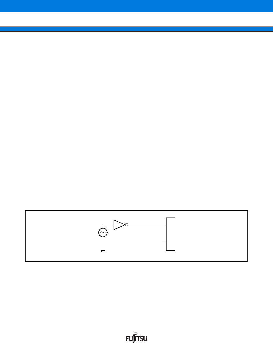
The following figure shows a sample use of external clock signals.
5.
Treatment of power supply pins (VCC/VSS)
In products with multiple VCC or VSS pins, the pins of the same potential are internally connected in the device
to avoid abnormal operations including latch-up. However, you must connect the pins to external power supply
and a ground line to lower the electro-magnetic emission level, to prevent abnormal operation of strobe signals
caused by the rise in the ground level, and to conform to the total output current rating. Moreover, connect the
current supply source with the VCC and VSS pins of this device at the low impedance.
It is also advisable to connect a ceramic bypass capacitor of approximately 0.1
μF between VCC pin and VSS pin
near this device.
X0
X1
OPEN
Using external clock
相关PDF资料 |
PDF描述 |
|---|---|
| MB90F395HAPMT | 16-BIT, FLASH, 24 MHz, MICROCONTROLLER, PQFP120 |
| MB90F428GBPFV | 16-BIT, FLASH, 16 MHz, MICROCONTROLLER, PQFP100 |
| MB90F423GBPFV | 16-BIT, FLASH, 16 MHz, MICROCONTROLLER, PQFP100 |
| MB90423GBPFV | 16-BIT, MROM, 16 MHz, MICROCONTROLLER, PQFP100 |
| MB90427GBPFV | 16-BIT, MROM, 16 MHz, MICROCONTROLLER, PQFP100 |
相关代理商/技术参数 |
参数描述 |
|---|---|
| MB90F334APMC1-GE1 | 制造商:FUJITSU 功能描述: |
| MB90F334APMC1-G-SPE1 | 制造商:FUJITSU 功能描述: |
| MB90F334APMC-G-JNE1 | 制造商:FUJITSU 功能描述: |
| MB90F334APMC-G-SNE1 | 制造商:FUJITSU 功能描述: |
| MB90F334APMC-G-SPE1 | 制造商:FUJITSU 功能描述: |
发布紧急采购,3分钟左右您将得到回复。