- 您现在的位置:买卖IC网 > PDF目录80564 > MB90F346CPF (FUJITSU LTD) 16-BIT, FLASH, 24 MHz, MICROCONTROLLER, PQFP100 PDF资料下载
参数资料
| 型号: | MB90F346CPF |
| 厂商: | FUJITSU LTD |
| 元件分类: | 微控制器/微处理器 |
| 英文描述: | 16-BIT, FLASH, 24 MHz, MICROCONTROLLER, PQFP100 |
| 封装: | PLASTIC, QFP-100 |
| 文件页数: | 6/76页 |
| 文件大小: | 1033K |
| 代理商: | MB90F346CPF |
第1页第2页第3页第4页第5页当前第6页第7页第8页第9页第10页第11页第12页第13页第14页第15页第16页第17页第18页第19页第20页第21页第22页第23页第24页第25页第26页第27页第28页第29页第30页第31页第32页第33页第34页第35页第36页第37页第38页第39页第40页第41页第42页第43页第44页第45页第46页第47页第48页第49页第50页第51页第52页第53页第54页第55页第56页第57页第58页第59页第60页第61页第62页第63页第64页第65页第66页第67页第68页第69页第70页第71页第72页第73页第74页第75页第76页
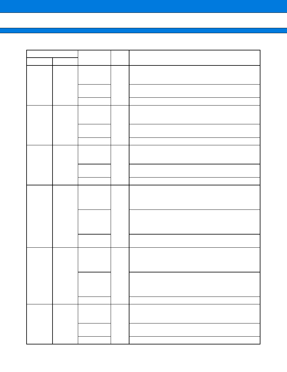
MB90340 Series
14
(Continued)
Pin No.
Pin name
Circuit
type
Function
LQFP100*2 QFP100*1
92
94
P15
G
General purpose I/O. The register can be set to select whether
to use a pull-up resistor. This function is enabled in single-chip
mode.
AD13
I/O pin for 13th bit of the external address/data bus.
This function is enabled when the external bus is enabled.
SIN4
Serial data input pin for UART4 (MB90V340 only)
93
95
P16
G
General purpose I/O. The register can be set to select whether
to use a pull-up resistor. This function is enabled in single-chip
mode.
AD14
I/O pin for 14th bit of the external address/data bus.
This function is enabled when the external bus is enabled.
SOT4
Serial data output pin for UART4 (MB90V340 only)
94
96
P17
G
General purpose I/O. The register can be set to select whether
to use a pull-up resistor. This function is enabled in single-chip
mode.
AD15
I/O pin for 15th bit of the external address/data bus. This func-
tion is enabled when the external bus is enabled.
SCK4
Clock I/O pin for UART4 (MB90V340 only)
95 to 98
97 to 100
P20 to P23
G
General purpose I/O. The register can be set to select whether
to use a pull-up resistor.In external bus mode, the pin is
enabled as a general-purpose I/O port when the corresponding
bit in the external address output control register (HACR) is 1.
A16 to A19
Output pins for A16 to A19 of the external address bus. When
the corresponding bit in the external address output control
register (HACR) is 0, the pins are enabled as high address
output pins (A16 to A19).
PPG9,PPGB,
PPGD,PPGF
Output pins for PPGs
99 to 2
1 to 4
P24 to P27
G
General purpose I/O. The register can be set to select whether
to use a pull-up resistor.In external bus mode, the pin is
enabled as a general-purpose I/O port when the corresponding
bit in the external address output control register (HACR) is 1.
A20 to A23
Output pins for A20 to A23 of the external address bus. When
the corresponding bit in the external address output control
register (HACR) is 0, the pins are enabled as high address
output pins (A20 to A23).
IN0 to IN3
Data sample input pins for input captures ICU0 to ICU3
35
P30
G
General purpose I/O.The register can be set to select whether
to use a pull-up resistor.This function is enabled in single-chip
mode.
ALE
Address latch enable output pin. This function is enabled when
the external bus is enabled.
IN4
Data sample input pin for input capture ICU4
相关PDF资料 |
PDF描述 |
|---|---|
| M41T315W-85MH6 | REAL TIME CLOCK, PDSO28 |
| MPC8245RVV400D | 32-BIT, 400 MHz, RISC PROCESSOR, PBGA352 |
| MB90F346CAPFV | 16-BIT, FLASH, 24 MHz, MICROCONTROLLER, PQFP100 |
| MC68HC705P6ADW | 8-BIT, OTPROM, 2.1 MHz, MICROCONTROLLER, PDSO28 |
| MC68HCP11E1CFU2 | 8-BIT, 2 MHz, MICROCONTROLLER, PQFP64 |
相关代理商/技术参数 |
参数描述 |
|---|---|
| MB90F347ASPMCR-GS-SPE2 | 制造商:FUJITSU 功能描述: |
| MB90F347CAPFR-GSE1 | 制造商:FUJITSU 功能描述: |
| MB90F347CAPFR-GS-SPE1 | 制造商:FUJITSU 功能描述: |
| MB90F347CASPF-GSE1 | 制造商:FUJITSU 功能描述:IC 16BIT MCU CAN 5V SMD QFP100 |
| MB90F347CASPFR-GSE1 | 制造商:FUJITSU 功能描述: |
发布紧急采购,3分钟左右您将得到回复。