- 您现在的位置:买卖IC网 > PDF目录69021 > MB90F523BPFV 16-BIT, FLASH, 16 MHz, MICROCONTROLLER, PQFP120 PDF资料下载
参数资料
| 型号: | MB90F523BPFV |
| 元件分类: | 微控制器/微处理器 |
| 英文描述: | 16-BIT, FLASH, 16 MHz, MICROCONTROLLER, PQFP120 |
| 封装: | PLASTIC, QFP-120 |
| 文件页数: | 10/99页 |
| 文件大小: | 978K |
| 代理商: | MB90F523BPFV |
第1页第2页第3页第4页第5页第6页第7页第8页第9页当前第10页第11页第12页第13页第14页第15页第16页第17页第18页第19页第20页第21页第22页第23页第24页第25页第26页第27页第28页第29页第30页第31页第32页第33页第34页第35页第36页第37页第38页第39页第40页第41页第42页第43页第44页第45页第46页第47页第48页第49页第50页第51页第52页第53页第54页第55页第56页第57页第58页第59页第60页第61页第62页第63页第64页第65页第66页第67页第68页第69页第70页第71页第72页第73页第74页第75页第76页第77页第78页第79页第80页第81页第82页第83页第84页第85页第86页第87页第88页第89页第90页第91页第92页第93页第94页第95页第96页第97页第98页第99页
MB90520A/520B Series
18
Connection of a bypass capacitor of approximately 0.1
F between VCC and VSS is recommended to prevent
power supply noise. Connect the capacitor close to the VCC and VSS pins.
Crystal oscillator circuit
Noise on the X0 and X1 pins can be a cause of device misoperation. Place the X0 and X1 pins, crystal oscillator
(or ceramic oscillator) , and bypass capacitor to ground as close together as possible. Also, design the circuit
board so that the X0 and X1 pin wiring does not cross other wiring.
Surrounding the X0/X1 and X0A/X1A pins with ground in the printed circuit board design is recommended to
ensure stable operation.
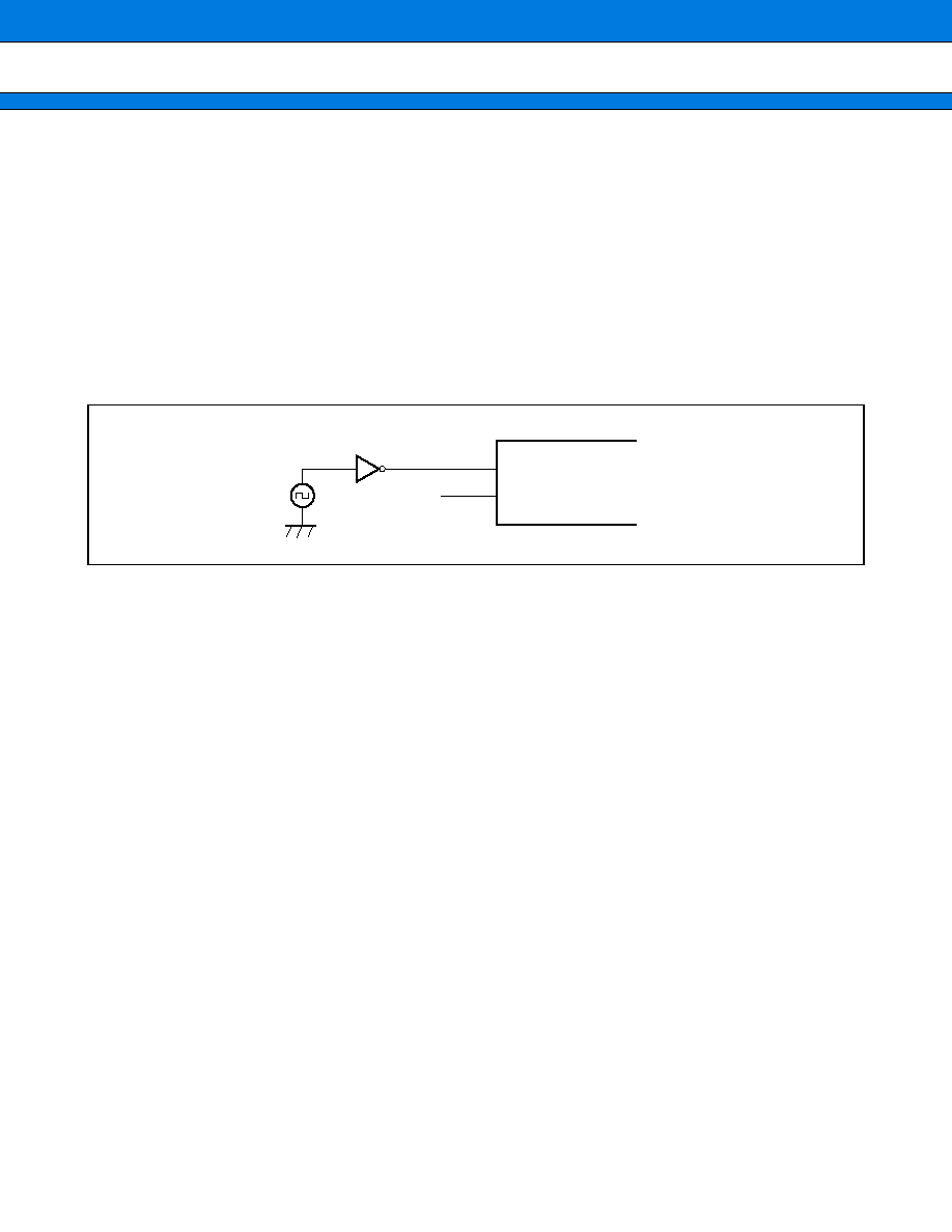
Notes on using an external clock
When using an external clock, drive the X0 pin only and leave the X1 pin open.
The figure below shows an example of how to use an external clock.
Precautions when not using sub-clock mode
Connect an oscillator to X0A and X1A, even if not using sub-clock mode.
Treatment of unused pins
Leaving unused input pins unconnected can cause misoperation or permanent damage to the device due to
latchup. Always pull-up or pull-down unused pins using a 2 k
or larger resistor.
If some I/O pins are unused, either set as outputs and leave open circuit or set as inputs and treat in the same
way as input pins.
Treatment of N.C. pins
Always leave N.C. (non connect) pins open circuit.
Treatment of pins when A/D converter not used
When not using the A/D converter and D/A converter, always connect AVCC
= DVCC = AVRH = VCC and AVSS =
AVRL
= VSS.
Sequence for connecting and disconnecting the A/D converter power supply and analog input pins
Do not apply voltage to the A/D and D/A converter power supply (AVCC, AVRH, AVRL, DVCC, DVSS) or analog
inputs (AN0 to AN7) until the digital power supply (VCC) is turned on.
When turning the device off, turn off the digital power supply after disconnecting the A/D converter power
supply and analog inputs. When turning the power on or off, ensure that AVRH and DVCC do not exceed AVCC
(turning the analog and digital power supplies on and off simultaneously is OK) .
Shared use of general-purpose I/O ports and LCD controller/driver SEG/COM pins
The SEG08 to SEG31 and COM0 to COM3 pins are shared with general-purpose I/O ports. The electrical
ratings for SEG08 to SEG23 and COM0 to COM3 are the same as for CMOS outputs and the electrical ratings
for SEG24 to SEG31 are the same as for N-ch open-drain ports.
X0
Open circuit
MB90520A/520B series
X1
Example of how to use an external clock
相关PDF资料 |
PDF描述 |
|---|---|
| MB90522APFF | 16-BIT, MROM, 16 MHz, MICROCONTROLLER, PQFP120 |
| MB90523APFF | 16-BIT, MROM, 16 MHz, MICROCONTROLLER, PQFP120 |
| MB90522BPFV | 16-BIT, MROM, 16 MHz, MICROCONTROLLER, PQFP120 |
| MB90522APFV | 16-BIT, MROM, 16 MHz, MICROCONTROLLER, PQFP120 |
| MB90523APFV | 16-BIT, MROM, 16 MHz, MICROCONTROLLER, PQFP120 |
相关代理商/技术参数 |
参数描述 |
|---|---|
| MB90F523BPM1R-GE1 | 制造商:FUJITSU 功能描述: |
| MB90F523BPMC1-GE1 | 制造商:FUJITSU 功能描述: |
| MB90F543GPF-GE1 | 功能描述:IC MCU 16BIT 制造商:cypress semiconductor corp 系列:F2MC-16LX MB90540G 包装:托盘 零件状态:在售 核心处理器:F2MC-16LX 核心尺寸:16-位 速度:16MHz 连接性:CAN,EBI/EMI,SCI,串行输入/输出,UART/USART 外设:POR,WDT I/O 数:81 程序存储容量:128KB(128K x 8) 程序存储器类型:闪存 EEPROM 容量:- RAM 容量:6K x 8 电压 - 电源(Vcc/Vdd):4.5 V ~ 5.5 V 数据转换器:A/D 8x8/10b 振荡器类型:外部 工作温度:-40°C ~ 105°C(TA) 封装/外壳:100-BQFP 供应商器件封装:100-PQFP(20x14) 标准包装:66 |
| MB90F543GPFR-GE1 | 制造商:FUJITSU 功能描述: |
| MB90F543GSPFR-GE1 | 制造商:FUJITSU 功能描述: |
发布紧急采购,3分钟左右您将得到回复。