- 您现在的位置:买卖IC网 > PDF目录378653 > MC100EL14DW (MOTOROLA INC) IC, 551001 128K X 8 ST. RA PDF资料下载
参数资料
| 型号: | MC100EL14DW |
| 厂商: | MOTOROLA INC |
| 元件分类: | 时钟及定时 |
| 英文描述: | IC, 551001 128K X 8 ST. RA |
| 中文描述: | 100EL SERIES, LOW SKEW CLOCK DRIVER, 5 TRUE OUTPUT(S), 0 INVERTED OUTPUT(S), PDSO20 |
| 封装: | PLASTIC, SOIC-20 |
| 文件页数: | 1/4页 |
| 文件大小: | 85K |
| 代理商: | MC100EL14DW |
SEMICONDUCTOR TECHNICAL DATA
4–1
REV 1
Motorola, Inc. 1996
7/95
The MC100LVEL/100EL14 is a low skew 1:5 clock distribution chip
designed explicitly for low skew clock distribution applications. The
device can be driven by either a differential or single-ended ECL or, if
positive power supplies are used, PECL input signal. The LVEL14 is
functionally and pin compatible with the EL14 but is designed to operate
in ECL or PECL mode for a voltage supply range of –3.0V to –3.8V ( or
3.0V to 3.8V). If a single-ended input is to be used the VBB output should
be connected to the CLK input and bypassed to ground via a 0.01
μ
F
capacitor. The VBB output is designed to act as the switching reference
for the input of the LVEL14 under single-ended input conditions, as a
result this pin can only source/sink up to 0.5mA of current.
The LVEL14 features a multiplexed clock input to allow for the
distribution of a lower speed scan or test clock along with the high speed
system clock. When LOW (or left open and pulled LOW by the input
pulldown resistor) the SEL pin will select the differential clock input.
The common enable (EN) is synchronous so that the outputs will only
be enabled/disabled when they are already in the LOW state. This avoids
any chance of generating a runt clock pulse when the device is
enabled/disabled as can happen with an asynchronous control. The
internal flip flop is clocked on the falling edge of the input clock, therefore
all associated specification limits are referenced to the negative edge of
the clock input.
50ps Output-to-Output Skew
Synchronous Enable/Disable
Multiplexed Clock Input
75k
Internal Input Pulldown Resistors
>2000V ESD Protection
VEE Range of –3.0V to –5.5V
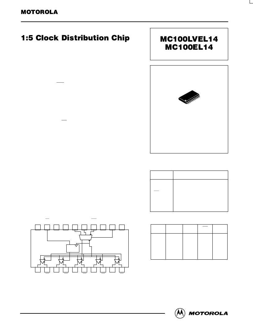
LOGIC DIAGRAM AND PINOUT ASSIGNMENT
Q1
Q2
Q3
Q4
17
18
16
15
14
13
12
4
3
5
6
7
8
9
VCC
11
10
Q4
Q3
Q2
Q1
NC
SCLK
CLK
CLK
VBB
SEL
VEE
D
Q
1 0
Q0
19
20
2
1
VCC
Q0
EN
DW SUFFIX
PLASTIC SOIC PACKAGE
CASE 751D-04
1
20
PIN
FUNCTION
CLK
SCLK
EN
SEL
VBB
Q0–4
Diff Clock Inputs
Scan Clock Input
Sync Enable
Clock Select Input
Reference Output
Diff Clock Outputs
PIN DESCRIPTION
CLK
L
H
X
X
X
SCLK
X
X
L
H
X
SEL
L
L
H
H
X
EN
L
L
L
L
H
Q
L
H
L
H
L*
FUNCTION TABLE
* On next negative transition of
CLK or SCLK
相关PDF资料 |
PDF描述 |
|---|---|
| MC100LVEL16D | Differential Receiver |
| MC10106FN | Triple 4-3-3-Input NOR Gate |
| MC10106 | Triple 4-3-3-Input NOR Gate |
| MC10106L | Triple 4-3-3-Input NOR Gate |
| MC10106P | Triple 4-3-3-Input NOR Gate |
相关代理商/技术参数 |
参数描述 |
|---|---|
| MC100EL14DWG | 功能描述:时钟驱动器及分配 5V ECL 1:5 Clock Distribution RoHS:否 制造商:Micrel 乘法/除法因子:1:4 输出类型:Differential 最大输出频率:4.2 GHz 电源电压-最大: 电源电压-最小:5 V 最大工作温度:+ 85 C 封装 / 箱体:SOIC-8 封装:Reel |
| MC100EL14DWG | 制造商:ON Semiconductor 功能描述:CLOCK GENERATOR / DISTRIBUTOR LOGIC IC |
| MC100EL14DWR2 | 功能描述:时钟驱动器及分配 5V ECL 1:5 Clock RoHS:否 制造商:Micrel 乘法/除法因子:1:4 输出类型:Differential 最大输出频率:4.2 GHz 电源电压-最大: 电源电压-最小:5 V 最大工作温度:+ 85 C 封装 / 箱体:SOIC-8 封装:Reel |
| MC100EL14DWR2G | 功能描述:时钟驱动器及分配 5V ECL 1:5 Clock Distribution RoHS:否 制造商:Micrel 乘法/除法因子:1:4 输出类型:Differential 最大输出频率:4.2 GHz 电源电压-最大: 电源电压-最小:5 V 最大工作温度:+ 85 C 封装 / 箱体:SOIC-8 封装:Reel |
| MC100EL15 | 制造商:ON Semiconductor 功能描述: |
发布紧急采购,3分钟左右您将得到回复。