参数资料
| 型号: | MC100EL14DWG |
| 厂商: | ON Semiconductor |
| 文件页数: | 1/9页 |
| 文件大小: | 0K |
| 描述: | IC CLK BUFF MUX 2:5 1GHZ 20-SOIC |
| 标准包装: | 38 |
| 系列: | 100EL |
| 类型: | 扇出缓冲器(分配),多路复用器 |
| 电路数: | 1 |
| 比率 - 输入:输出: | 2:5 |
| 差分 - 输入:输出: | 是/是 |
| 输入: | ECL,PECL |
| 输出: | ECL,PECL |
| 频率 - 最大: | 1GHz |
| 电源电压: | 4.2 V ~ 5.7 V |
| 工作温度: | -40°C ~ 85°C |
| 安装类型: | 表面贴装 |
| 封装/外壳: | 20-SOIC(0.295",7.50mm 宽) |
| 供应商设备封装: | 20-SOIC |
| 包装: | 管件 |
| 其它名称: | MC100EL14DWGOS |
Semiconductor Components Industries, LLC, 2008
November, 2008 Rev. 8
1
Publication Order Number:
MC100EL14/D
MC100EL14
5V ECL 1:5 Clock
Distribution Chip
The MC100EL14 is a low skew 1:5 clock distribution chip designed
explicitly for low skew clock distribution applications. The VBB pin, an
internally generated voltage supply, is available to this device only.
For single-ended input conditions, the unused differential input is
connected to VBB as a switching reference voltage. VBB may also
rebias AC coupled inputs. When used, decouple VBB and VCC via a
0.01
mF capacitor and limit current sourcing or sinking to 0.5 mA.
When not used, VBB should be left open.
The EL14 features a multiplexed clock input to allow for the
distribution of a lower speed scan or test clock along with the high
speed system clock. When LOW (or left open and pulled LOW by the
input pulldown resistor) the SEL pin will select the differential clock
input.
The common enable (EN) is synchronous so that the outputs will only
be enabled/disabled when they are already in the LOW state. This
avoids any chance of generating a runt clock pulse when the device is
enabled/disabled as can happen with an asynchronous control. The
internal flip flop is clocked on the falling edge of the input clock,
therefore all associated specification limits are referenced to the
negative edge of the clock input.
Features
50 ps Output-to-Output Skew
Synchronous Enable/Disable
Multiplexed Clock Input
The 100 Series Contains Temperature Compensation
PECL Mode Operating Range: VCC = 4.2 V to 5.7 V
with VEE = 0 V
NECL Mode Operating Range: VCC = 0 V
with VEE = 4.2 V to 5.7 V
Q Output will Default LOW with Inputs Open or at VEE
Internal Input Pulldown Resistors on All Inputs, Pullup Resistors
on Inverted Inputs
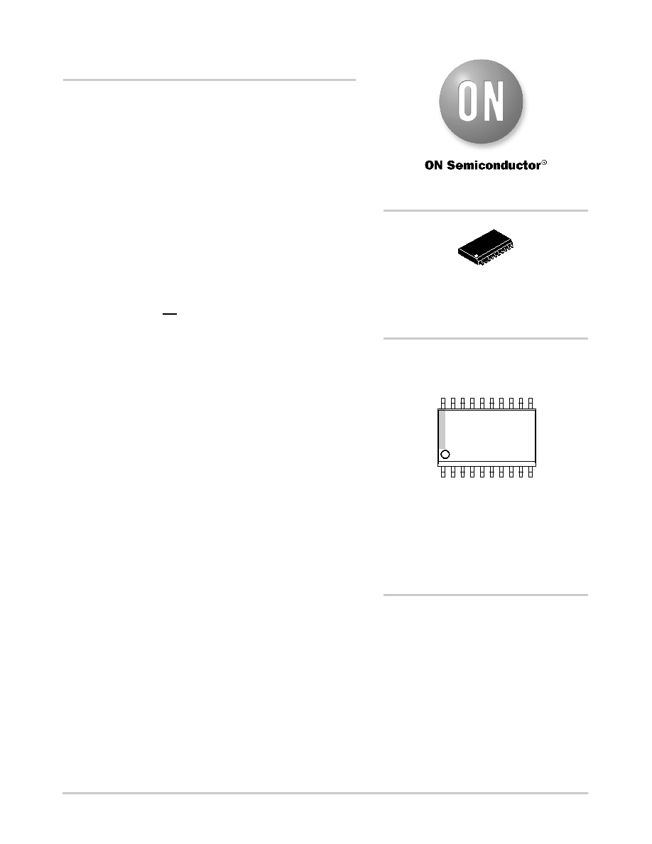
SOIC20L
DW SUFFIX
CASE 751D
MARKING DIAGRAM
http://onsemi.com
A
= Assembly Location
WL
= Wafer Lot
YY
= Year
WW
= Work Week
G
= PbFree Package
20
1
100EL14
AWLYYWWG
*For additional marking information, refer to
Application Note AND8002/D.
See detailed ordering and shipping information in the package
dimensions section on page 7 of this data sheet.
ORDERING INFORMATION
相关PDF资料 |
PDF描述 |
|---|---|
| V150A24H500BG2 | CONVERTER MOD DC/DC 24V 500W |
| V150A28H500BL3 | CONVERTER MOD DC/DC 28V 500W |
| VI-J72-MY | CONVERTER MOD DC/DC 15V 50W |
| VI-J71-MY | CONVERTER MOD DC/DC 12V 50W |
| VI-J5K-MY | CONVERTER MOD DC/DC 40V 50W |
相关代理商/技术参数 |
参数描述 |
|---|---|
| MC100EL14DWG | 制造商:ON Semiconductor 功能描述:CLOCK GENERATOR / DISTRIBUTOR LOGIC IC |
| MC100EL14DWR2 | 功能描述:时钟驱动器及分配 5V ECL 1:5 Clock RoHS:否 制造商:Micrel 乘法/除法因子:1:4 输出类型:Differential 最大输出频率:4.2 GHz 电源电压-最大: 电源电压-最小:5 V 最大工作温度:+ 85 C 封装 / 箱体:SOIC-8 封装:Reel |
| MC100EL14DWR2G | 功能描述:时钟驱动器及分配 5V ECL 1:5 Clock Distribution RoHS:否 制造商:Micrel 乘法/除法因子:1:4 输出类型:Differential 最大输出频率:4.2 GHz 电源电压-最大: 电源电压-最小:5 V 最大工作温度:+ 85 C 封装 / 箱体:SOIC-8 封装:Reel |
| MC100EL15 | 制造商:ON Semiconductor 功能描述: |
| MC100EL15D | 功能描述:时钟驱动器及分配 5V ECL 1:4 Clock RoHS:否 制造商:Micrel 乘法/除法因子:1:4 输出类型:Differential 最大输出频率:4.2 GHz 电源电压-最大: 电源电压-最小:5 V 最大工作温度:+ 85 C 封装 / 箱体:SOIC-8 封装:Reel |
发布紧急采购,3分钟左右您将得到回复。