参数资料
| 型号: | MC100EP195BMNR4G |
| 厂商: | ON Semiconductor |
| 文件页数: | 4/17页 |
| 文件大小: | 0K |
| 描述: | IC DELAY LINE 1024TAP 32-QFN |
| 标准包装: | 1 |
| 系列: | 100EP |
| 标片/步级数: | 1024 |
| 功能: | 可编程 |
| 延迟到第一抽头: | 2.5ns |
| 接头增量: | 10ps |
| 可用的总延迟: | 2.2ns ~ 12.2ns |
| 独立延迟数: | 1 |
| 电源电压: | 3 V ~ 3.6 V |
| 工作温度: | -40°C ~ 85°C |
| 安装类型: | 表面贴装 |
| 封装/外壳: | 32-VFQFN 裸露焊盘 |
| 供应商设备封装: | 32-QFN(5x5) |
| 包装: | 剪切带 (CT) |
| 其它名称: | MC100EP195BMNR4GOSCT |
MC100EP195B
http://onsemi.com
12
VEE
D0
VCC
Q
NC
VCC
CASCADE
EN
SETMAX
V
CC
V
EE
LEN
D2 D1
CASCADE
SETMIN
VBB
IN
VEE
D8
VEF
D3
D4
D5
D6
D7
D9
D10
IN
VCF
INPUT
OUTPUT
VEE
D0
VCC
Q
NC
VCC
CASCADE
EN
SETMAX
V
CC
V
EE
LEN
D2 D1
CASCADE
SETMIN
VBB
IN
VEE
D8
VEF
D3
D4
D5
D6
D7
D9
D10
IN
VCF
EP195B
CHIP #2
EP195B
CHIP #1
ADDRESS BUS
A11 A10 A9 A8 A7 A6 A5 A4 A3 A2 A1 A0
Need if Chip #3 is used
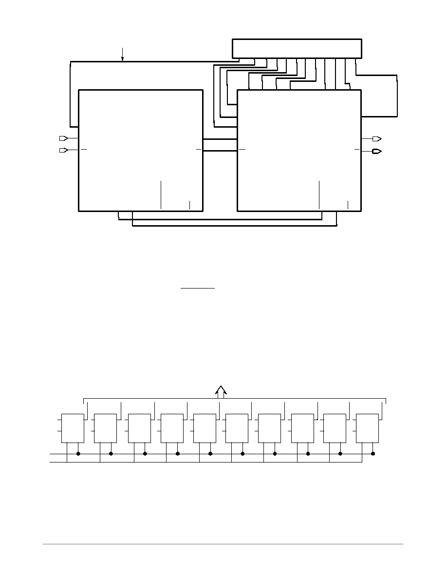
Figure 5. Cascading Interconnect Architecture
An expansion of the latch section of the block diagram is
pictured in Figure 6. Use of this diagram will simplify the
explanation of how the cascade circuitry works. When D10
of chip #1 in Figure 5 is LOW this device’s
CASCADE output will also be low while the CASCADE
output will be high. In this condition the SET MIN pin of
chip #2 will be asserted HIGH and thus all of the latches of
chip #2 will be reset and the device will be set at its minimum
delay.
Chip #1, on the other hand, will have both SET MIN and
SET MAX deasserted so that its delay will be controlled
entirely by the address bus A0—A9. If the delay needed is
greater than can be achieved with 1023 gate delays
(1111111111 on the A0—A9 address bus) D10 will be
asserted to signal the need to cascade the delay to the next
EP195B device. When D10 is asserted, the SET MIN pin of
chip #2 will be deasserted and SET MAX pin asserted
resulting in the device delay to be the maximum delay.
Table 11 shows the delay time of two EP195B chips in
cascade.
To expand this cascading scheme to more devices, one
simply needs to connect the D10 pin from the next chip to
the address bus and CASCADE outputs to the next chip in
the same manner as pictured in Figure 5. The only addition
to the logic is the increase of one line to the address bus for
cascade control of the second programmable delay chip.
SET
MIN
SET
MAX
TO SELECT MULTIPLEXERS
BIT 0
D0 Q0
LEN
Set Reset
BIT 1
D1 Q1
LEN
Set Reset
BIT 2
D2 Q2
LEN
Set Reset
BIT 3
D3 Q3
LEN
Set Reset
BIT 4
D4 Q4
LEN
Set Reset
BIT 5
D5 Q5
LEN
Set Reset
BIT 6
D6 Q6
LEN
Set Reset
BIT 7
D7 Q7
LEN
Set Reset
BIT 8
D8 Q8
LEN
Set Reset
BIT 9
D9 Q9
LEN
Set Reset
Figure 6. Expansion of the Latch Section of the EP195B Block Diagram
相关PDF资料 |
PDF描述 |
|---|---|
| VI-22X-MW | CONVERTER MOD DC/DC 5.2V 100W |
| MS3120E16-23P | CONN RCPT 23POS WALL MNT W/PINS |
| VE-B5H-IU-F1 | CONVERTER MOD DC/DC 52V 200W |
| LTC6994MPS6-2#TRPBF | IC DELAY LINE SOT-23-6 |
| VE-BWD-MW-B1 | CONVERTER MOD DC/DC 85V 100W |
相关代理商/技术参数 |
参数描述 |
|---|---|
| MC100EP195FA | 功能描述:延迟线/计时元素 3.3V/5V ECL RoHS:否 制造商:Micrel 功能:Active Programmable Delay Line 传播延迟时间:1000 ps 工作温度范围: 封装 / 箱体:QFN-24 封装:Tube |
| MC100EP195FAG | 功能描述:延迟线/计时元素 3.3V/5V ECL Programmable Delay RoHS:否 制造商:Micrel 功能:Active Programmable Delay Line 传播延迟时间:1000 ps 工作温度范围: 封装 / 箱体:QFN-24 封装:Tube |
| MC100EP195FAG | 制造商:ON Semiconductor 功能描述:DELAY LINE IC |
| MC100EP195FAR2 | 功能描述:延迟线/计时元素 3.3V/5V ECL RoHS:否 制造商:Micrel 功能:Active Programmable Delay Line 传播延迟时间:1000 ps 工作温度范围: 封装 / 箱体:QFN-24 封装:Tube |
| MC100EP195FAR2G | 功能描述:延迟线/计时元素 3.3V/5V ECL Programmable Delay RoHS:否 制造商:Micrel 功能:Active Programmable Delay Line 传播延迟时间:1000 ps 工作温度范围: 封装 / 箱体:QFN-24 封装:Tube |
发布紧急采购,3分钟左右您将得到回复。