参数资料
| 型号: | MC100EP809MNR4G |
| 厂商: | ON Semiconductor |
| 文件页数: | 1/10页 |
| 文件大小: | 0K |
| 描述: | IC CLOCK BUFFER MUX 1:9 32-QFN |
| 标准包装: | 1,000 |
| 系列: | 100EP |
| 类型: | 扇出缓冲器(分配),多路复用器 |
| 电路数: | 2 |
| 比率 - 输入:输出: | 1:9 |
| 差分 - 输入:输出: | 是/是 |
| 输入: | HSTL,LVDS,LVPECL |
| 输出: | HSTL |
| 频率 - 最大: | 750MHz |
| 电源电压: | 3 V ~ 3.6 V |
| 工作温度: | 0°C ~ 85°C |
| 安装类型: | 表面贴装 |
| 封装/外壳: | 32-VFQFN 裸露焊盘 |
| 供应商设备封装: | 32-QFN(5x5) |
| 包装: | 带卷 (TR) |
Semiconductor Components Industries, LLC, 2008
May, 2008 Rev. 9
1
Publication Order Number:
MC100EP809/D
MC100EP809
3.3V1:9 Differential
HSTL/PECL/LVDS to HSTL
Clock Driver with LVTTL
Clock Select and Enable
Description
The MC100EP809 is a low skew 1to9 differential clock driver,
designed with clock distribution in mind, accepting two clock sources
into an input multiplexer. The part is designed for use in low voltage
applications which require a large number of outputs to drive precisely
aligned low skew signals to their destination. The two clock inputs are
one differential HSTL and one differential LVPECL. Both input pairs
can accept LVDS levels. They are selected by the CLK_SEL pin
which is LVTTL. To avoid generation of a runt clock pulse when the
device is enabled/disabled, the Output Enable (OE), which is LVTTL,
is synchronous ensuring the outputs will only be enabled/disabled
when they are already in LOW state (Figure 9).
The MC100EP809 guarantees low outputtooutput skew. The
optimal design, layout, and processing minimize skew within a device
and from lot to lot. The MC100EP809 output structure uses open
emitter architecture and will be terminated with 50
W to ground
instead of a standard HSTL configuration (Figure 7). To ensure the
tight skew specification is realized, both sides of the differential output
need to be terminated identically into 50
W even if only one output is
being used. If an output pair is unused, both outputs may be left open
(unterminated) without affecting skew.
Designers can take advantage of the EP809’s performance to
distribute low skew clocks across the backplane of the board. Both
clock inputs may be singleend driven by biasing the nondriven pin
in an input pair (Figure 8).
Features
100 ps Typical DevicetoDevice Skew
15 ps Typical within Device Skew
HSTL Compatible Outputs Drive 50 W to GND with no
Offset Voltage
Maximum Frequency > 750 MHz
850 ps Typical Propagation Delay
Fully Compatible with Micrel SY89809L
PECL and HSTL Mode Operating Range: VCCI = 3 V to 3.6 V
with GND = 0 V, VCCO = 1.6 V to 2.0 V
Open Input Default State
PbFree Packages are Available
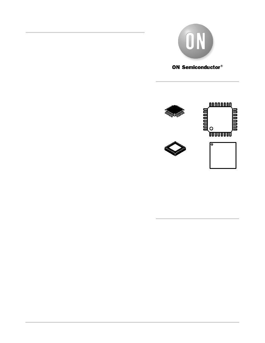
32
1
MC100
AWLYYWWG
EP809
32LEAD LQFP
FA SUFFIX
CASE 873A
MARKING
DIAGRAMS*
A
= Assembly Location
WL
= Wafer Lot
YY
= Year
WW
= Work Week
G or G = PbFree Package
(Note: Microdot may be in either location)
*For additional marking information, refer to
Application Note AND8002/D.
See detailed ordering and shipping information in the package
dimensions section on page 8 of this data sheet.
ORDERING INFORMATION
http://onsemi.com
32
1
MC100
EP809
AWLYYWWG
G
1
QFN32
MN SUFFIX
CASE 488AM
相关PDF资料 |
PDF描述 |
|---|---|
| VE-J73-MY | CONVERTER MOD DC/DC 24V 50W |
| V375A36H400B | CONVERTER MOD DC/DC 36V 400W |
| V375A36H400BG3 | CONVERTER MOD DC/DC 36V 400W |
| AD9750ARZRL | IC DAC 10BIT 125MSPS 28SOIC |
| V375A36H400BG2 | CONVERTER MOD DC/DC 36V 400W |
相关代理商/技术参数 |
参数描述 |
|---|---|
| MC100EP89D | 制造商:ONSEMI 制造商全称:ON Semiconductor 功能描述:Evaluation Board Manual for High Frequency SOIC 8 |
| MC100EP90 | 制造商:ONSEMI 制造商全称:ON Semiconductor 功能描述:-3.3V / -5V Triple ECL Input to LVPECL/PECL Output Translator |
| MC100EP90DT | 功能描述:转换 - 电压电平 3.3V/5V Triple ECL RoHS:否 制造商:Micrel 类型:CML/LVDS/LVPECL to LVCMOS/LVTTL 传播延迟时间:1.9 ns 电源电流:14 mA 电源电压-最大:3.6 V 电源电压-最小:3 V 最大工作温度:+ 85 C 安装风格:SMD/SMT 封装 / 箱体:MLF-8 |
| MC100EP90DTG | 功能描述:转换 - 电压电平 3.3V/5V Triple ECL to LVPECL/PECL RoHS:否 制造商:Micrel 类型:CML/LVDS/LVPECL to LVCMOS/LVTTL 传播延迟时间:1.9 ns 电源电流:14 mA 电源电压-最大:3.6 V 电源电压-最小:3 V 最大工作温度:+ 85 C 安装风格:SMD/SMT 封装 / 箱体:MLF-8 |
| MC100EP90DTR2 | 功能描述:转换 - 电压电平 3.3V/5V Triple ECL RoHS:否 制造商:Micrel 类型:CML/LVDS/LVPECL to LVCMOS/LVTTL 传播延迟时间:1.9 ns 电源电流:14 mA 电源电压-最大:3.6 V 电源电压-最小:3 V 最大工作温度:+ 85 C 安装风格:SMD/SMT 封装 / 箱体:MLF-8 |
发布紧急采购,3分钟左右您将得到回复。