- 您现在的位置:买卖IC网 > PDF目录8960 > MC100ES60T23EF (IDT, Integrated Device Technology Inc)IC XLATOR LV PECL DUAL 8-SOIC PDF资料下载
参数资料
| 型号: | MC100ES60T23EF |
| 厂商: | IDT, Integrated Device Technology Inc |
| 文件页数: | 4/8页 |
| 文件大小: | 0K |
| 描述: | IC XLATOR LV PECL DUAL 8-SOIC |
| 标准包装: | 97 |
| 系列: | 100ES |
| 逻辑功能: | 变换器 |
| 位数: | 2 |
| 输入类型: | LVPECL |
| 输出类型: | LVTTL |
| 通道数: | 2 |
| 输出/通道数目: | 1 |
| 差分 - 输入:输出: | 是/无 |
| 传输延迟(最大): | 1.75ns |
| 电源电压: | 3 V ~ 3.6 V |
| 工作温度: | -40°C ~ 85°C |
| 封装/外壳: | 8-SOIC(0.154",3.90mm 宽) |
| 供应商设备封装: | 8-SOIC |
| 包装: | 管件 |
| 其它名称: | 800-2225 MC100ES60T23EF-ND |
MC100ES60T23 REVISION 3 DECEMBER 14, 2012
4
2012 Integrated Device Technology, Inc.
MC100ES60T23 DATA SHEET
3.3V DUAL DIFFERENTIAL LVPECL TO LVTTL TRANSLATOR
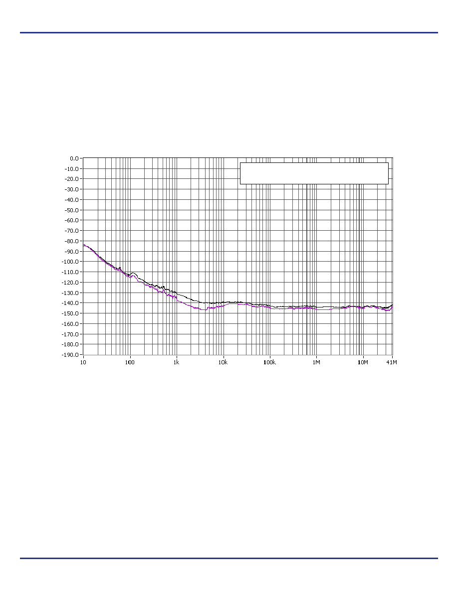
ADDITIVE PHASE JITTER
The spectral purity in a band at a specific offset from the
fundamental compared to the power of the fundamental is
called the dBc Phase Noise. This value is normally expressed
using a Phase noise plot and is most often the specified plot
in many applications. Phase noise is defined as the ratio of
the noise power present in a 1Hz band at a specified offset
from the fundamental frequency to the power value of the
fundamental. This ratio is expressed in decibels (dBm) or a
ratio of the power in the 1Hz band to the power in the
fundamental. When the required offset is specified, the phase
noise is called a dBc value, which simply means dBm at a
specified offset from the fundamental. By investigating jitter in
the frequency domain, we get a better understanding of its
effects on the desired application over the entire time record
of the signal. It is mathematically possible to calculate an
expected bit error rate given a phase noise plot.
As with most timing specifications, phase noise
measurements have issues. The primary issue relates to the
limitations of the equipment. Often the noise floor of the
equipment is higher than the noise floor of the device. This is
illustrated above. The device meets the noise floor of what is
shown, but can actually be lower. The phase noise is
dependant on the input source and measurement equipment.
Offset From Carrier Frequency (Hz)
SSB
Ph
ase
No
is
edBc
/Hz
Additive Phase Jitter
@ 156.25MHz (12kHz-20MHz) = 0.18ps typical
相关PDF资料 |
PDF描述 |
|---|---|
| VE-24K-MY-F1 | CONVERTER MOD DC/DC 40V 50W |
| LTC2604IGN-1#PBF | IC DAC 16BIT QUAD R-R 16-SSOP |
| LTC2604IGN#PBF | IC DAC 16BIT QUAD R-R OUT 16SSOP |
| GTC06CF-32-82P | CONN PLUG 16POS STRAIGHT W/PINS |
| M83723/85G1212N | CONN RCPT 12POS JAM NUT W/PINS |
相关代理商/技术参数 |
参数描述 |
|---|---|
| MC100ES60T23EFR2 | 功能描述:时钟发生器及支持产品 FSL Diff. LVPECL to LVTTL/LVCMOS Trans. RoHS:否 制造商:Silicon Labs 类型:Clock Generators 最大输入频率:14.318 MHz 最大输出频率:166 MHz 输出端数量:16 占空比 - 最大:55 % 工作电源电压:3.3 V 工作电源电流:1 mA 最大工作温度:+ 85 C 安装风格:SMD/SMT 封装 / 箱体:QFN-56 |
| MC100ES6111AC | 功能描述:时钟缓冲器 Buffer RoHS:否 制造商:Texas Instruments 输出端数量:5 最大输入频率:40 MHz 传播延迟(最大值): 电源电压-最大:3.45 V 电源电压-最小:2.375 V 最大功率耗散: 最大工作温度:+ 85 C 最小工作温度:- 40 C 封装 / 箱体:LLP-24 封装:Reel |
| MC100ES6111ACR2 | 功能描述:时钟缓冲器 FSL 1-10 Diff LVPECL Fanout Buffer RoHS:否 制造商:Texas Instruments 输出端数量:5 最大输入频率:40 MHz 传播延迟(最大值): 电源电压-最大:3.45 V 电源电压-最小:2.375 V 最大功率耗散: 最大工作温度:+ 85 C 最小工作温度:- 40 C 封装 / 箱体:LLP-24 封装:Reel |
| MC100ES6111FA | 功能描述:时钟缓冲器 Buffer RoHS:否 制造商:Texas Instruments 输出端数量:5 最大输入频率:40 MHz 传播延迟(最大值): 电源电压-最大:3.45 V 电源电压-最小:2.375 V 最大功率耗散: 最大工作温度:+ 85 C 最小工作温度:- 40 C 封装 / 箱体:LLP-24 封装:Reel |
| MC100ES6111FAR2 | 功能描述:IC CLOCK BUFFER MUX 2:10 32-LQFP RoHS:否 类别:集成电路 (IC) >> 时钟/计时 - 时钟缓冲器,驱动器 系列:100ES 标准包装:1 系列:HiPerClockS™ 类型:扇出缓冲器(分配),多路复用器 电路数:1 比率 - 输入:输出:2:18 差分 - 输入:输出:是/无 输入:CML,LVCMOS,LVPECL,LVTTL,SSTL 输出:LVCMOS,LVTTL 频率 - 最大:250MHz 电源电压:2.375 V ~ 3.465 V 工作温度:0°C ~ 70°C 安装类型:表面贴装 封装/外壳:32-LQFP 供应商设备封装:32-TQFP(7x7) 包装:- 其它名称:800-1923-6 |
发布紧急采购,3分钟左右您将得到回复。