- 您现在的位置:买卖IC网 > PDF目录181331 > MC100ES6210AC (飞思卡尔半导体(中国)有限公司) Low Voltage 2.5/3.3 V Differential ECL/PECL/HSTL Fanout Buffer PDF资料下载
参数资料
| 型号: | MC100ES6210AC |
| 厂商: | 飞思卡尔半导体(中国)有限公司 |
| 英文描述: | Low Voltage 2.5/3.3 V Differential ECL/PECL/HSTL Fanout Buffer |
| 中文描述: | 低电压2.5/3.3 V差动ECL / PECL的/ HSTL扇出缓冲器 |
| 文件页数: | 3/8页 |
| 文件大小: | 226K |
| 代理商: | MC100ES6210AC |
Advanced Clock Drivers Devices
Freescale Semiconductor
3
MC100ES6210
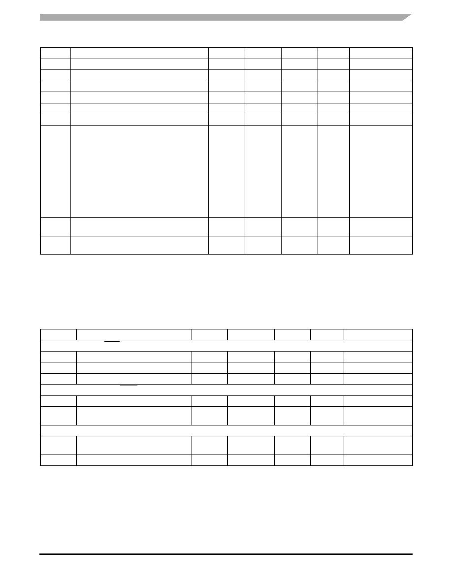
Table 3. General Specifications
Symbol
Characteristics
Min
Typ
Max
Unit
Condition
VTT
Output Termination Voltage
VCC – 2(1)
1. Output termination voltage VTT = 0 V for VCC = 2.5 V operation is supported but the power consumption of the device will increase.
V
MM
ESD Protection (Machine Model)
200
V
HBM
ESD Protection (Human Body Model)
2000
V
CDM
ESD Protection (Charged Device Model)
V
LU
Latch-Up Immunity
200
mA
CIN
Input Capacitance
4.0
pF
Inputs
θJA
Thermal Resistance Junction to Ambient
JESD 51-3, single layer test board
JESD 51-6, 2S2P multilayer test board
83.1
73.3
68.9
63.8
57.4
59.0
54.4
52.5
50.4
47.8
86.0
75.4
70.9
65.3
59.6
60.6
55.7
53.8
51.5
48.8
°C/W
Natural convection
100 ft/min
200 ft/min
400 ft/min
800 ft/min
Natural convection
100 ft/min
200 ft/min
400 ft/min
800 ft/min
θJC
Thermal Resistance Junction to Case
23.0
26.3
°C/W
MIL-SPEC 883E
Method 1012.1
TJ
Operating Junction Temperature(2)
(continuous operation)
MTBF = 9.1 years
2. Operating junction temperature impacts device life time. Maximum continuous operating junction temperature should be selected according
to the application life time requirements (See application note AN1545 for more information). The device AC and DC parameters are
specified up to 110
°C junction temperature allowing the MC100ES6210 to be used in applications requiring industrial temperature range. It
is recommended that users of the MC100ES6210 employ thermal modeling analysis to assist in applying the junction temperature
specifications to their particular application.
110
°C
Table 4. PECL DC Characteristics (VCC = 2.5 V ± 5% or VCC = 3.3 V ± 5%, VEE = GND, TJ = 0°C to +110°C)
Symbol
Characteristics
Min
Typ
Max
Unit
Condition
Clock Input Pair CLKA, CLKA, CLKB, CLKB (PECL differential signals)
VPP
Differential Input Voltage(1)
1. VPP (DC) is the minimum differential input voltage swing required to maintain device functionality.
0.1
1.3
V
Differential operation
VCMR
Differential Cross Point Voltage(2)
2. VCMR (DC) is the crosspoint of the differential input signal. Functional operation is obtained when the crosspoint is within the VCMR (DC)
range and the input swing lies within the VPP (DC) specification.
1.0
VCC – 0.3
V
Differential operation
IIN
Input Current(1)
±100
AVIN = VIL or VIN = VIH
PECL Clock Outputs (QA0-4, QA0-4, QB0-4, QB0-4)
VOH
Output High Voltage
VCC –1.2
VCC –1.005
VCC –0.7
V
IOH = –30 mA(3)
3. Equivalent to a termination of 50
to VTT.
VOL
Output Low Voltage
VCC = 3.3 V±5%
VCC = 2.5 V±5%
VCC –1.9
VCC –1.705
VCC –1.5
VCC –1.3
VIOL = –5 mA(3)
Supply Current and VBB
IEE
Maximum Quiescent Supply Current
without Output Termination Current
60
100
mA
VEE pin
VBB
Output Reference Voltage
VCC –1.38
VCC –1.26
VCC –1.14
V
IBB = 0.2 mA
相关PDF资料 |
PDF描述 |
|---|---|
| MC100LVEL58MNR4 | 100LVEL SERIES, 2 LINE TO 1 LINE MULTIPLEXER, COMPLEMENTARY OUTPUT, PDSO8 |
| MC100 | 1 CHANNEL TRANSISTOR OUTPUT OPTOCOUPLER |
| MC10E336FNR2 | 10E SERIES, 3-BIT REGISTERED TRANSCEIVER, INVERTED OUTPUT, PQCC28 |
| MC10EP56DW | 10E SERIES, DUAL 2 LINE TO 1 LINE MULTIPLEXER, COMPLEMENTARY OUTPUT, PDSO20 |
| MC10H109P | 10H SERIES, DUAL 5-INPUT OR/NOR GATE, PDIP16 |
相关代理商/技术参数 |
参数描述 |
|---|---|
| MC100ES6210ACR2 | 功能描述:时钟缓冲器 FSL 1-5 Dual Diff LVPECL Fanout Buffer RoHS:否 制造商:Texas Instruments 输出端数量:5 最大输入频率:40 MHz 传播延迟(最大值): 电源电压-最大:3.45 V 电源电压-最小:2.375 V 最大功率耗散: 最大工作温度:+ 85 C 最小工作温度:- 40 C 封装 / 箱体:LLP-24 封装:Reel |
| MC100ES6210FA | 功能描述:时钟缓冲器 Buffer RoHS:否 制造商:Texas Instruments 输出端数量:5 最大输入频率:40 MHz 传播延迟(最大值): 电源电压-最大:3.45 V 电源电压-最小:2.375 V 最大功率耗散: 最大工作温度:+ 85 C 最小工作温度:- 40 C 封装 / 箱体:LLP-24 封装:Reel |
| MC100ES6210KLF | 功能描述:IC CLOCK BUFFER 1:5 3GHZ 32VFQFN RoHS:是 类别:集成电路 (IC) >> 时钟/计时 - 时钟缓冲器,驱动器 系列:100ES 标准包装:74 系列:- 类型:扇出缓冲器(分配) 电路数:1 比率 - 输入:输出:1:10 差分 - 输入:输出:是/是 输入:HCSL, LVCMOS, LVDS, LVPECL, LVTTL 输出:HCSL,LVDS 频率 - 最大:400MHz 电源电压:3 V ~ 3.6 V 工作温度:-40°C ~ 85°C 安装类型:表面贴装 封装/外壳:32-VFQFN 裸露焊盘 供应商设备封装:32-QFN(5x5) 包装:管件 |
| MC100ES6220AE | 功能描述:时钟缓冲器 FSL Dual 1-10 Diff LVPECL Fanout Buffer RoHS:否 制造商:Texas Instruments 输出端数量:5 最大输入频率:40 MHz 传播延迟(最大值): 电源电压-最大:3.45 V 电源电压-最小:2.375 V 最大功率耗散: 最大工作温度:+ 85 C 最小工作温度:- 40 C 封装 / 箱体:LLP-24 封装:Reel |
| MC100ES6220AER2 | 功能描述:IC CLK BUFFER 1:10 1GHZ 52-LQFP RoHS:是 类别:集成电路 (IC) >> 时钟/计时 - 时钟缓冲器,驱动器 系列:100ES 标准包装:74 系列:- 类型:扇出缓冲器(分配) 电路数:1 比率 - 输入:输出:1:10 差分 - 输入:输出:是/是 输入:HCSL, LVCMOS, LVDS, LVPECL, LVTTL 输出:HCSL,LVDS 频率 - 最大:400MHz 电源电压:3 V ~ 3.6 V 工作温度:-40°C ~ 85°C 安装类型:表面贴装 封装/外壳:32-VFQFN 裸露焊盘 供应商设备封装:32-QFN(5x5) 包装:管件 |
发布紧急采购,3分钟左右您将得到回复。