- 您现在的位置:买卖IC网 > PDF目录2093 > MC100ES6254AC (IDT, Integrated Device Technology Inc)IC CLK BUFF MUX 2:6 3GHZ 32-LQFP PDF资料下载
参数资料
| 型号: | MC100ES6254AC |
| 厂商: | IDT, Integrated Device Technology Inc |
| 文件页数: | 6/12页 |
| 文件大小: | 0K |
| 描述: | IC CLK BUFF MUX 2:6 3GHZ 32-LQFP |
| 标准包装: | 250 |
| 系列: | 100ES |
| 类型: | 扇出缓冲器(分配),多路复用器 |
| 电路数: | 1 |
| 比率 - 输入:输出: | 2:6 |
| 差分 - 输入:输出: | 是/是 |
| 输入: | LVCMOS,LVPECL |
| 输出: | LVPECL |
| 频率 - 最大: | 3GHz |
| 电源电压: | 2.375 V ~ 3.465 V |
| 工作温度: | 0°C ~ 70°C |
| 安装类型: | 表面贴装 |
| 封装/外壳: | 32-LQFP |
| 供应商设备封装: | 32-TQFP(7x7) |
| 包装: | 托盘 |
MC100ES6254 REV. 7 JANUARY 7, 2013
3
2013 Integrated Device Technology, Inc.
MC100ES6254 Data Sheet
2.5/3.3V DIFFERENTIAL LVPECL 2X2 CLOCK SWITCH AND FANOUT BUFFER
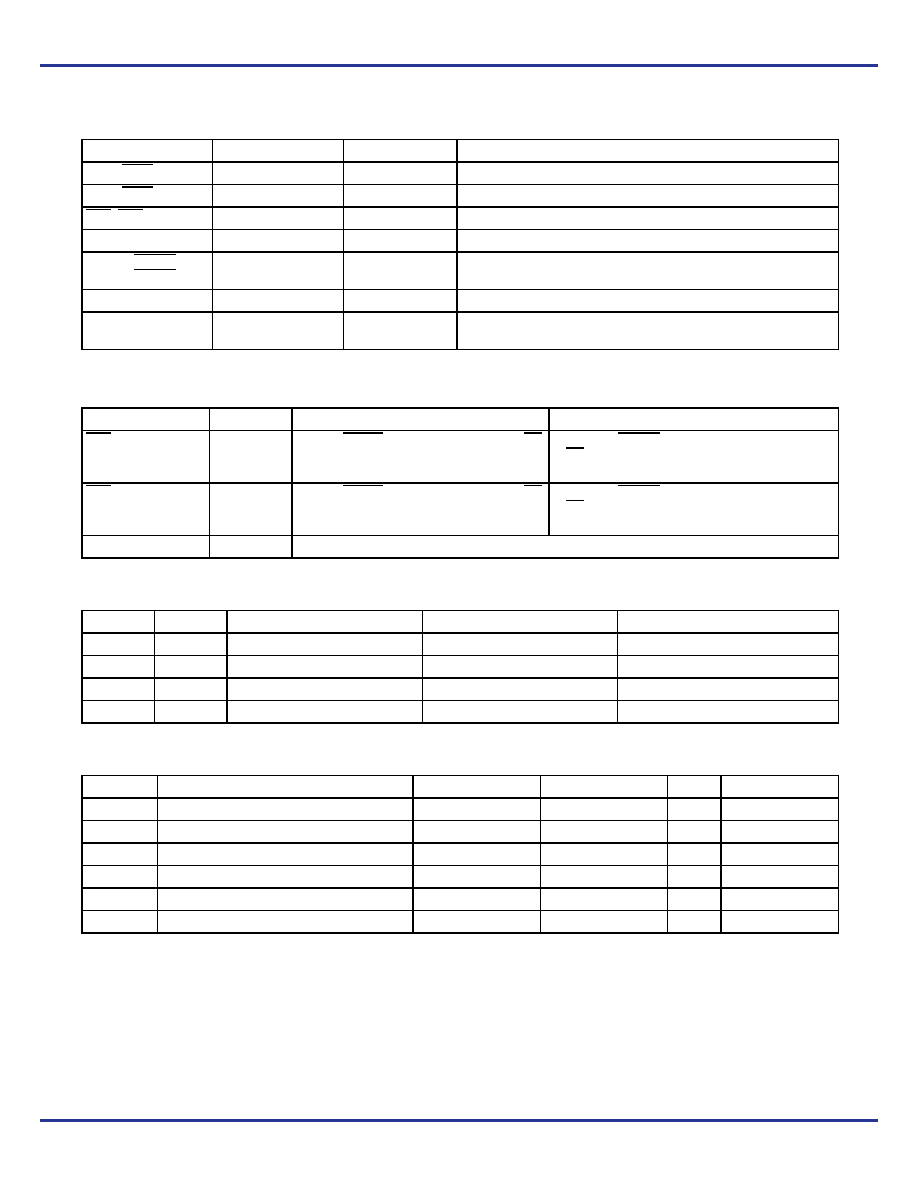
Table 1. Pin Configuration
Pin
I/O
Type
Function
CLK0, CLK0
Input
LVPECL
Differential reference clock signal input 0
CLK1, CLK1
Input
LVPECL
Differential reference clock signal input 1
OEA, OEB
Input
LVCMOS
Output enable
SEL0, SEL1
Input
LVCMOS
Clock switch select
QA[0-2], QA[0-2]
QB[0-2], QB[0-2]
Output
LVPECL
Differential clock outputs (banks A and B)
GND
Supply
GND
Negative power supply
VCC
Supply
VCC
Positive power supply. All VCC pins must be connected to the positive
power supply for correct DC and AC operation
Table 2. Function Table
Control
Default
0
1
OEA
0
QA[0-2], Qx[0-2] are active. Deassertion of OE
can be asynchronous to the reference clock
without generation of output runt pulses
QA[0-2] = L, QA[0-2] = H (outputs disabled). Assertion
of OE can be asynchronous to the reference clock
without generation of output runt pulses
OEB
0
QA[0-2], Qx[0-2] are active. Deassertion of OE
can be asynchronous to the reference clock
without generation of output runt pulses
QA[0-2] = L, QA[0-2] = H (outputs disabled). Assertion
of OE can be asynchronous to the reference clock
without generation of output runt pulses
SEL0, SEL1
00
Refer to Table 4
Table 3. Clock Select Control
SEL0
SEL1
CLK0 Routed to
CLK1 Routed to
Application Mode
0
QA[0:2] and QB[0:2]
—
1:6 fanout of CLK0
0
1
—
QA[0:2] and QB[0:2]
1:6 fanout of CLK1
1
0
QA[0:2]
QB[0:2]
Dual 1:3 buffer
1
QB[0:2]
QA[0:2]
Dual 1:3 buffer (crossed)
Table 4. Absolute Maximum Ratings(1)
1. Absolute maximum continuous ratings are those maximum values beyond which damage to the device may occur. Exposure to these
conditions or conditions beyond those indicated may adversely affect device reliability. Functional operation at absolute-maximum-rated
conditions is not implied.
Symbol
Characteristics
Min
Max
Unit
Condition
VCC
Supply Voltage
-0.3
3.6
V
VIN
DC Input Voltage
-0.3
VCC+0.3
V
VOUT
DC Output Voltage
-0.3
VCC+0.3
V
IIN
DC Input Current
20
mA
IOUT
DC Output Current
50
mA
TS
Storage Temperature
-65
125
C
相关PDF资料 |
PDF描述 |
|---|---|
| MC100ES6535EJ | IC CLOCK BUFFER MUX 2:4 20-TSSOP |
| MC100ES8111AC | IC CLOCK BUFFER MUX 2:10 32-LQFP |
| MC100LVE222FAR2G | IC CLK BUFF DVDR MUX 2:15 52LQFP |
| MC100LVE310FNR2 | IC CLK BUFF MUX 2:8 1GHZ 28-PLCC |
| MC100LVEL01DTR2 | IC GATE OR/NOR ECL 4INPUT 8TSSOP |
相关代理商/技术参数 |
参数描述 |
|---|---|
| MC100ES6254ACR2 | 功能描述:时钟驱动器及分配 FSL Differential LVP ECL 2x2 Clock Switch RoHS:否 制造商:Micrel 乘法/除法因子:1:4 输出类型:Differential 最大输出频率:4.2 GHz 电源电压-最大: 电源电压-最小:5 V 最大工作温度:+ 85 C 封装 / 箱体:SOIC-8 封装:Reel |
| MC100ES6254FA | 功能描述:时钟缓冲器 Buffer RoHS:否 制造商:Texas Instruments 输出端数量:5 最大输入频率:40 MHz 传播延迟(最大值): 电源电压-最大:3.45 V 电源电压-最小:2.375 V 最大功率耗散: 最大工作温度:+ 85 C 最小工作温度:- 40 C 封装 / 箱体:LLP-24 封装:Reel |
| MC100ES6535DT | 功能描述:IC CLOCK BUFFER MUX 2:4 20-TSSOP RoHS:否 类别:集成电路 (IC) >> 时钟/计时 - 时钟缓冲器,驱动器 系列:100ES 标准包装:1 系列:HiPerClockS™ 类型:扇出缓冲器(分配),多路复用器 电路数:1 比率 - 输入:输出:2:18 差分 - 输入:输出:是/无 输入:CML,LVCMOS,LVPECL,LVTTL,SSTL 输出:LVCMOS,LVTTL 频率 - 最大:250MHz 电源电压:2.375 V ~ 3.465 V 工作温度:0°C ~ 70°C 安装类型:表面贴装 封装/外壳:32-LQFP 供应商设备封装:32-TQFP(7x7) 包装:- 其它名称:800-1923-6 |
| MC100ES6535EJ | 功能描述:时钟驱动器及分配 FSL 1-4 LVCMOS to LV PECL Fanout Buffer RoHS:否 制造商:Micrel 乘法/除法因子:1:4 输出类型:Differential 最大输出频率:4.2 GHz 电源电压-最大: 电源电压-最小:5 V 最大工作温度:+ 85 C 封装 / 箱体:SOIC-8 封装:Reel |
| MC100ES6535EJR2 | 功能描述:时钟驱动器及分配 FSL 1-4 LVCMOS to LV PECL Fanout Buffer RoHS:否 制造商:Micrel 乘法/除法因子:1:4 输出类型:Differential 最大输出频率:4.2 GHz 电源电压-最大: 电源电压-最小:5 V 最大工作温度:+ 85 C 封装 / 箱体:SOIC-8 封装:Reel |
发布紧急采购,3分钟左右您将得到回复。