- 您现在的位置:买卖IC网 > PDF目录8686 > MC100LVE310FNR2G (ON Semiconductor)IC CLK BUFF MUX 2:8 1GHZ 28-PLCC PDF资料下载
参数资料
| 型号: | MC100LVE310FNR2G |
| 厂商: | ON Semiconductor |
| 文件页数: | 4/7页 |
| 文件大小: | 0K |
| 描述: | IC CLK BUFF MUX 2:8 1GHZ 28-PLCC |
| 标准包装: | 1 |
| 系列: | 100LVE |
| 类型: | 扇出缓冲器(分配),多路复用器 |
| 电路数: | 1 |
| 比率 - 输入:输出: | 2:8 |
| 差分 - 输入:输出: | 是/是 |
| 输入: | LVECL,LVPECL |
| 输出: | LVECL,LVPECL |
| 频率 - 最大: | 1GHz |
| 电源电压: | 3 V ~ 3.8 V |
| 工作温度: | -40°C ~ 85°C |
| 安装类型: | 表面贴装 |
| 封装/外壳: | 28-LCC(J 形引线) |
| 供应商设备封装: | 28-PLCC(11.51x11.51) |
| 包装: | 剪切带 (CT) |
| 其它名称: | MC100LVE310FNR2GOSCT |
MC100LVE310
http://onsemi.com
4
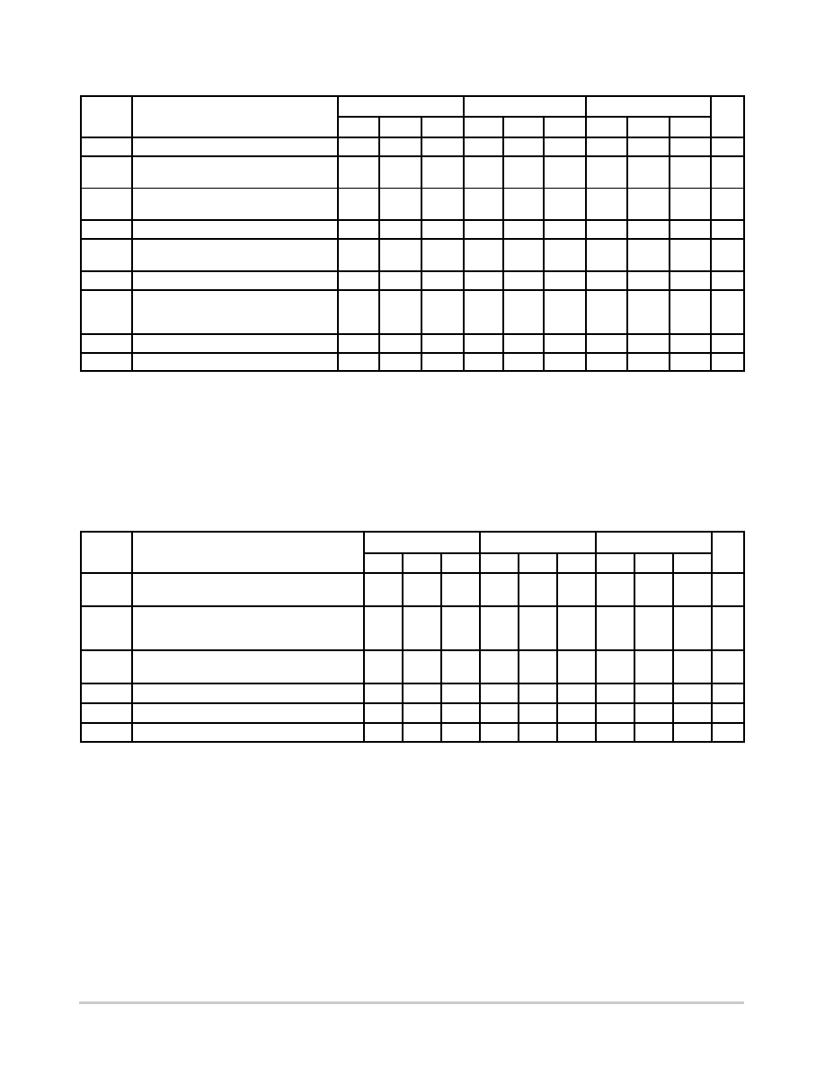
Symbol
Characteristic
-40
°C
25
°C
85
°C
Unit
Min
Typ
Max
Min
Typ
Max
Min
Typ
Max
IEE
Power Supply Current
55
60
55
60
65
70
mA
VOH
Output HIGH Voltage (Note 6)
-1085
-1005
-880
-102
5
-955
-880
-1025
-955
-880
mV
VOL
Output LOW Voltage (Note 6)
-1830
-1695
-1555
-181
0
-170
5
-1620
-1810
-1705
-1620
mV
VIH
Input HIGH Voltage (Single-Ended)
-1165
-880
-1165
-880
-1165
-880
mV
VIL
Input LOW Voltage (Single-Ended)
-1810
-1475
-181
0
-1475
-1810
-1475
mV
VBB
Output Voltage Reference
-1.38
-1.26
-1.38
-1.26
-1.38
-1.26
V
VIHCMR
Input HIGH Voltage Common Mode
Range (Differential Configuration)
(Note 7)
-1.5
-0.4
-1.5
-0.4
-1.5
-0.4
V
IIH
Input HIGH Current
150
mA
IIL
Input LOW Current
0.5
mA
NOTE: Device will meet the specifications after thermal equilibrium has been established when mounted in a test socket or printed circuit
board with maintained transverse airflow greater than 500 lfpm. Electrical parameters are guaranteed only over the declared
operating temperature range. Functional operation of the device exceeding these conditions is not implied. Device specification limit
values are applied individually under normal operating conditions and not valid simultaneously.
5. Input and output parameters vary 1:1 with VCC. VEE can vary ± 0.3 V.
6. Outputs are terminated through a 50
W resistor to VCC - 2 V.
7. VIHCMR min varies 1:1 with VEE, max varies 1:1 with VCC. VIHCMR is defined as the range within which the VIH level may vary, with the device
still meeting the propagation delay specification. The VIL level must be such that the peak to peak voltage is less than 1.0 V and greater than
or equal to VPP(min).
Symbol
Characteristic
-40
°C
25
°C
85
°C
Unit
Min
Typ
Max
Min
Typ
Max
Min
Typ
Max
fmax
Maximum Toggle Frequency @ Vout >500
mVpp
0.5
1.0
0.5
1.0
0.5
1.0
GHz
tPLH
tPHL
Propagation Delay to Output
IN (Differential Configuration) (Note 9)
IN (Single-Ended) (Note 10)
525
500
725
750
550
750
800
575
600
775
850
ps
tskew
Within-Device Skew (Note 11)
Part-to-Part Skew (Differential Configuration)
75
250
50
200
50
200
ps
tJITTER
Additive CLOCK Jitter (RMS) <0.5 GHz
1.5
2.0
1.5
2.0
1.5
2.0
ps
VPP
Input Swing (Note12)
500
1000
500
1000
500
1000
mV
tr/tf
Output Rise/Fall Time (20%-80%)
200
600
200
600
200
600
ps
NOTE: Device will meet the specifications after thermal equilibrium has been established when mounted in a test socket or printed circuit
board with maintained transverse airflow greater than 500 lfpm. Electrical parameters are guaranteed only over the declared
operating temperature range. Functional operation of the device exceeding these conditions is not implied. Device specification limit
values are applied individually under normal operating conditions and not valid simultaneously.
8.
VEE can vary ± 0.3 V.
9. The differential propagation delay is defined as the delay from the crossing points of the differential input signals to the crossing point of the
differential output signals.
10. The single‐ended propagation delay is defined as the delay from the 50% point of the input signal to the 50% point of the output signal.
11. The within-device skew is defined as the worst case difference between any two similar delay paths within a single device.
12. VPP(min) is defined as the minimum input differential voltage which will cause no increase in the propagation delay. The VPP(min) is AC limited
for the LVE310 as a differential input as low as 50 mV will still produce full ECL levels at the output.
相关PDF资料 |
PDF描述 |
|---|---|
| VI-JWH-MY | CONVERTER MOD DC/DC 52V 50W |
| V48A48H500B | CONVERTER MOD DC/DC 48V 500W |
| V375A12H400B2 | CONVERTER MOD DC/DC 12V 400W |
| VI-JWD-MY | CONVERTER MOD DC/DC 85V 50W |
| V48A36H500BG3 | CONVERTER MOD DC/DC 36V 500W |
相关代理商/技术参数 |
参数描述 |
|---|---|
| MC100LVEL01D | 功能描述:逻辑门 3.3V ECL 4-Input RoHS:否 制造商:Texas Instruments 产品:OR 逻辑系列:LVC 栅极数量:2 线路数量(输入/输出):2 / 1 高电平输出电流:- 16 mA 低电平输出电流:16 mA 传播延迟时间:3.8 ns 电源电压-最大:5.5 V 电源电压-最小:1.65 V 最大工作温度:+ 125 C 安装风格:SMD/SMT 封装 / 箱体:DCU-8 封装:Reel |
| MC100LVEL01DG | 功能描述:逻辑门 3.3V ECL 4-Input OR/NOR RoHS:否 制造商:Texas Instruments 产品:OR 逻辑系列:LVC 栅极数量:2 线路数量(输入/输出):2 / 1 高电平输出电流:- 16 mA 低电平输出电流:16 mA 传播延迟时间:3.8 ns 电源电压-最大:5.5 V 电源电压-最小:1.65 V 最大工作温度:+ 125 C 安装风格:SMD/SMT 封装 / 箱体:DCU-8 封装:Reel |
| MC100LVEL01DR2 | 功能描述:逻辑门 3.3V ECL 4-Input RoHS:否 制造商:Texas Instruments 产品:OR 逻辑系列:LVC 栅极数量:2 线路数量(输入/输出):2 / 1 高电平输出电流:- 16 mA 低电平输出电流:16 mA 传播延迟时间:3.8 ns 电源电压-最大:5.5 V 电源电压-最小:1.65 V 最大工作温度:+ 125 C 安装风格:SMD/SMT 封装 / 箱体:DCU-8 封装:Reel |
| MC100LVEL01DR2G | 功能描述:逻辑门 3.3V ECL 4-Input OR/NOR RoHS:否 制造商:Texas Instruments 产品:OR 逻辑系列:LVC 栅极数量:2 线路数量(输入/输出):2 / 1 高电平输出电流:- 16 mA 低电平输出电流:16 mA 传播延迟时间:3.8 ns 电源电压-最大:5.5 V 电源电压-最小:1.65 V 最大工作温度:+ 125 C 安装风格:SMD/SMT 封装 / 箱体:DCU-8 封装:Reel |
| MC100LVEL01DT | 功能描述:逻辑门 3.3V ECL 4-Input RoHS:否 制造商:Texas Instruments 产品:OR 逻辑系列:LVC 栅极数量:2 线路数量(输入/输出):2 / 1 高电平输出电流:- 16 mA 低电平输出电流:16 mA 传播延迟时间:3.8 ns 电源电压-最大:5.5 V 电源电压-最小:1.65 V 最大工作温度:+ 125 C 安装风格:SMD/SMT 封装 / 箱体:DCU-8 封装:Reel |
发布紧急采购,3分钟左右您将得到回复。