- 您现在的位置:买卖IC网 > PDF目录9700 > MC100LVEP16DTR2 (ON Semiconductor)IC RECEIVER/DRVR DIFF ECL 8TSSOP PDF资料下载
参数资料
| 型号: | MC100LVEP16DTR2 |
| 厂商: | ON Semiconductor |
| 文件页数: | 10/12页 |
| 文件大小: | 0K |
| 描述: | IC RECEIVER/DRVR DIFF ECL 8TSSOP |
| 产品变化通告: | Product Obsolescence 11/Feb/2009 |
| 标准包装: | 2,500 |
| 系列: | 100LVEP |
| 逻辑类型: | 差分接收器/驱动器 |
| 电源电压: | 2.375 V ~ 3.8 V |
| 工作温度: | -40°C ~ 85°C |
| 安装类型: | 表面贴装 |
| 封装/外壳: | 8-TSSOP,8-MSOP(0.118",3.00mm 宽) |
| 供应商设备封装: | 8-TSSOP |
| 包装: | 带卷 (TR) |
MC10LVEP16, MC100LVEP16
http://onsemi.com
7
Table 10. AC CHARACTERISTICS VCC = 0 V; VEE = 3.8 V to 2.375 V or VCC = 2.375 V to 3.8 V; VEE = 0 V (Note 27)
Symbol
Characteristic
40°C
25°C
85°C
Unit
Min
Typ
Max
Min
Typ
Max
Min
Typ
Max
fmax
Maximum Frequency
> 4
GHz
tPLH,
tPHL
Propagation Delay to
Output Differential
150
220
300
170
240
320
190
260
330
ps
tSKEW
Duty Cycle Skew (Note 28)
5.0
20
5.0
20
5.0
20
ps
tJITTER
CLOCK Random Jitter (RMS)
@ v 1.0 GHz
@ v 1.5 GHz
@ v 2.0 GHz
@ v 2.5 GHz
@ v 3.0 GHz
@ v 3.5 GHz
0.134
0.077
0.115
0.117
0.122
0.123
0.2
0.147
0.104
0.141
0.132
0.143
0.145
0.3
0.166
0.145
0.153
0.156
0.177
0.202
0.3
ps
VPP
Input Voltage Swing
(Differential Configuration)
150
800
1200
150
800
1200
150
800
1200
mV
tr
tf
Output Rise/Fall Times
Q, Q
(20% 80%)
70
120
170
80
130
180
100
150
200
ps
NOTE: Device will meet the specifications after thermal equilibrium has been established when mounted in a test socket or printed circuit
board with maintained transverse airflow greater than 500 lfpm. Electrical parameters are guaranteed only over the declared
operating temperature range. Functional operation of the device exceeding these conditions is not implied. Device specification limit
values are applied individually under normal operating conditions and not valid simultaneously.
27.Measured using a 750 mV source, 50% duty cycle clock source. All loading with 50 W to VCC 2.0 V.
28.Skew is measured between outputs under identical transitions. Duty cycle skew is defined only for differential operation when the delays
are measured from the cross point of the inputs to the cross point of the outputs.
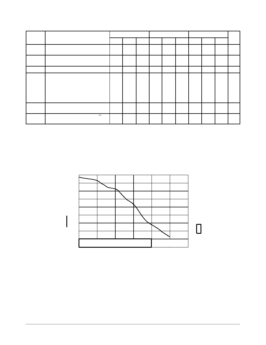
0
100
200
300
400
500
600
700
800
900
0
1000
2000
3000
4000
5000
6000
FREQUENCY (MHz)
1
2
3
4
5
6
7
8
(JITTER)
Figure 2. Fmax/Jitter
9
V
OUTpp
(mV)
JITTER
OUT
ps
(RMS)
相关PDF资料 |
PDF描述 |
|---|---|
| MS3121E12-10PW | CONN RCPT 10POS CBL MNT W/PINS |
| VI-251-IW-B1 | CONVERTER MOD DC/DC 12V 100W |
| MS3121E12-10P | CONN RCPT 10POS CBL MNT W/PINS |
| MC100LVEP16DR2 | IC RECEIVER/DRVR DIFF ECL 8-SOIC |
| VI-24V-IW-B1 | CONVERTER MOD DC/DC 5.8V 100W |
相关代理商/技术参数 |
参数描述 |
|---|---|
| MC100LVEP16DTR2G | 功能描述:总线收发器 2.5V/3.3V ECL Diff RoHS:否 制造商:Fairchild Semiconductor 逻辑类型:CMOS 逻辑系列:74VCX 每芯片的通道数量:16 输入电平:CMOS 输出电平:CMOS 输出类型:3-State 高电平输出电流:- 24 mA 低电平输出电流:24 mA 传播延迟时间:6.2 ns 电源电压-最大:2.7 V, 3.6 V 电源电压-最小:1.65 V, 2.3 V 最大工作温度:+ 85 C 封装 / 箱体:TSSOP-48 封装:Reel |
| MC100LVEP16MNR4 | 功能描述:总线收发器 2.5V/3.3V ECL Diff RoHS:否 制造商:Fairchild Semiconductor 逻辑类型:CMOS 逻辑系列:74VCX 每芯片的通道数量:16 输入电平:CMOS 输出电平:CMOS 输出类型:3-State 高电平输出电流:- 24 mA 低电平输出电流:24 mA 传播延迟时间:6.2 ns 电源电压-最大:2.7 V, 3.6 V 电源电压-最小:1.65 V, 2.3 V 最大工作温度:+ 85 C 封装 / 箱体:TSSOP-48 封装:Reel |
| MC100LVEP16MNR4G | 功能描述:总线收发器 2.5V/3.3V ECL Diff RoHS:否 制造商:Fairchild Semiconductor 逻辑类型:CMOS 逻辑系列:74VCX 每芯片的通道数量:16 输入电平:CMOS 输出电平:CMOS 输出类型:3-State 高电平输出电流:- 24 mA 低电平输出电流:24 mA 传播延迟时间:6.2 ns 电源电压-最大:2.7 V, 3.6 V 电源电压-最小:1.65 V, 2.3 V 最大工作温度:+ 85 C 封装 / 箱体:TSSOP-48 封装:Reel |
| MC100LVEP210FA | 功能描述:时钟缓冲器 2.5V/3.3V 1:5 Dual RoHS:否 制造商:Texas Instruments 输出端数量:5 最大输入频率:40 MHz 传播延迟(最大值): 电源电压-最大:3.45 V 电源电压-最小:2.375 V 最大功率耗散: 最大工作温度:+ 85 C 最小工作温度:- 40 C 封装 / 箱体:LLP-24 封装:Reel |
| MC100LVEP210FAG | 功能描述:时钟缓冲器 2.5V/3.3V 1:5 Dual ECL/PECL/HST Driver RoHS:否 制造商:Texas Instruments 输出端数量:5 最大输入频率:40 MHz 传播延迟(最大值): 电源电压-最大:3.45 V 电源电压-最小:2.375 V 最大功率耗散: 最大工作温度:+ 85 C 最小工作温度:- 40 C 封装 / 箱体:LLP-24 封装:Reel |
发布紧急采购,3分钟左右您将得到回复。