- 您现在的位置:买卖IC网 > PDF目录371001 > MC10E211 (ON SEMICONDUCTOR) Replaced by TPS2055A : 0.345A, 2.7-5.5V Single Hi-Side MOSFET, Fault Report, Act-High Enable 8-PDIP -40 to 85 PDF资料下载
参数资料
| 型号: | MC10E211 |
| 厂商: | ON SEMICONDUCTOR |
| 英文描述: | Replaced by TPS2055A : 0.345A, 2.7-5.5V Single Hi-Side MOSFET, Fault Report, Act-High Enable 8-PDIP -40 to 85 |
| 中文描述: | 1:6差分时钟分配芯片 |
| 文件页数: | 4/7页 |
| 文件大小: | 101K |
| 代理商: | MC10E211 |
MC10E211 MC100E211
MOTOROLA
ECLinPS and ECLinPS Lite
DL140 — Rev 4
2–4
APPLICATIONS INFORMATION
General Description
The MC10E/100E211 is a 1:6 fanout tree designed
explicitly for low skew high speed clock distribution. The
device was targeted to work in conjunction with the E111
device to provide another level of flexibility in the design and
implementation of clock distribution trees. The individual
synchronous enable controls and multiplexed clock inputs
make the device ideal as the first level distribution unit in a
distribution tree. The device provides the ability to distribute a
lower speed scan or test clock along with the high speed
system clock to ease the design of system diagnostics and
self test procedures. The individual enables could be used to
allow for the disabling of individual cards on a backplane in
fault tolerant designs.
Because of lower fanout and larger skews the E211 will
not likely be used as an alternative to the E111 for the bulk of
the clock fanout generation. Figure 1 shows a typical
application combining the two devices to take advantage of
the strengths of each.
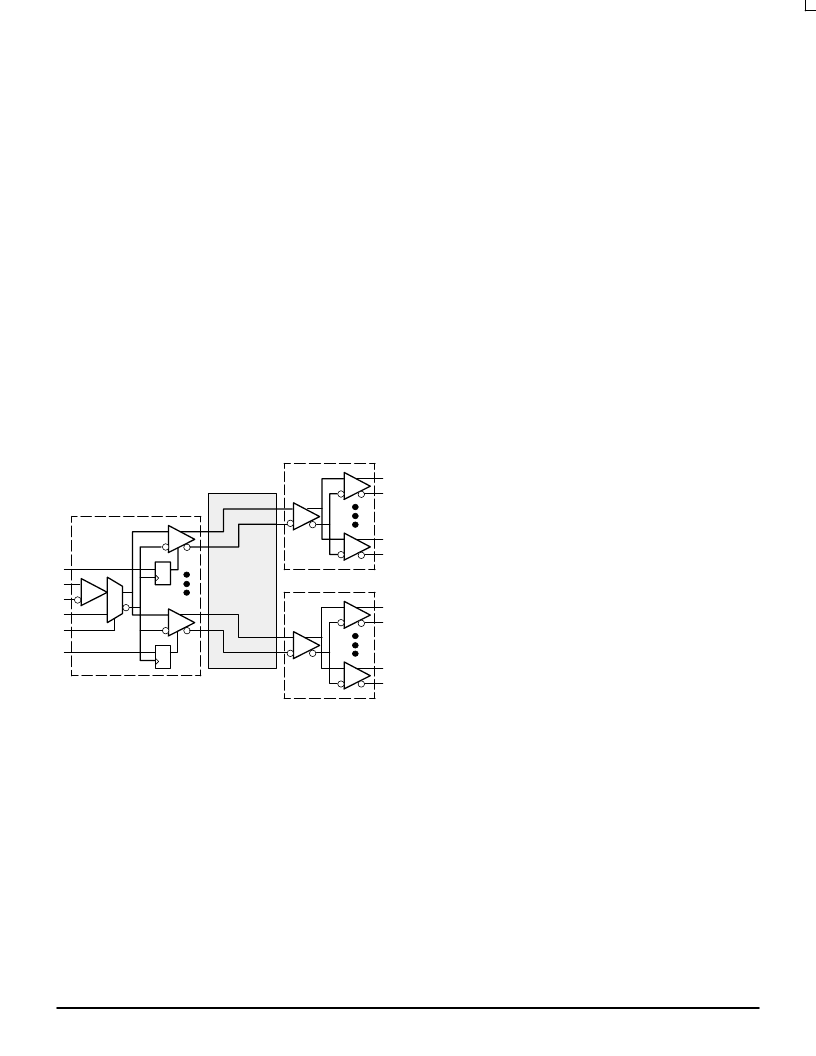
Figure 1. Standard E211 Application
E111
Q8
Q0
E211
Q5
Q0
E111
Q8
Q0
B
Using the E211 in PECL Designs
The E211 device can be utilized very effectively in designs
utilizing only a +5V power supply. Since the internal switching
reference levels are biased off of the VCC supply the input
thresholds for the single-ended inputs will vary with VCC. As a
result the single-ended inputs should be driven by a device
on the same board as the E211. Driving these inputs across a
backplane where significant differences between the VCC’s of
the transmitter and receiver can occur can lead to AC
performance and/or significant noise margin degradations.
Because the differential I/O does not use a switching
reference, and due to the CMR range of the E211, even
under worst case VCC situations between cards there will be
no AC performance or noise margin loss for the differential
CLK inputs.
For situations where TTL clocks are required the E211 can
be interfaced with the H641 or H643 ECL to TTL Clock
Distribution Chips from Motorola. The H641 is a single supply
1:9 PECL to TTL device while the H643 is a 1:8 dual supply
standard ECL to TTL device. By combining the superior skew
performance of the E211, or E111, with the low skew
translating capabilities of the H641 and H643 very low skew
TTL clock distribution networks can be realized.
Handling Open Inputs and Outputs
All of the input pins of the E211 have a 50k
to 75k
pulldown resistor to pull the input to VEE when left open. This
feature can cause a problem if the differential clock inputs are
left open as the input gate current source transistor will
become saturated. Under these conditions the outputs of the
CLK input buffer will go to an undefined state. It is
recommended, if possible,that the SCLK input should be
selected any time the differential CLK inputs are allowed to
float. The SCLK buffer, under open input conditions, will
maintain a defined output state and thus the Q outputs of the
device will be in a defined state (Q = LOW). Note that if all of
the inputs are left open the differential CLK input will be
selected and the state of the Q outputs will be undefined.
With the simultaneous switching characteristics and the
tight skew specifications of the E211 the handling of the
unused outputs becomes critical. To minimize the noise
generated on the die all outputs should be terminated in
pairs, ie. both the true and compliment outputs should be
terminated even if only one of the outputs will be used in the
system. With both complimentary pairs terminated the
current in the VCC pins will remain essentially constant and
thus inductance induced voltage glitches on VCC will not
occur. VCC glitches will result in distorted output waveforms
and degradations in the skew performance of the device.
The package parasitics of the 28-lead PLCC cause the
signals on a given pin to be influenced by signals on adjacent
pins. The E211 is characterized and tested with all of the
outputs switching, therefore the numbers in the data book are
guaranteed only for this situation. If all of the outputs of the
E211 are not needed and there is a desire to save power the
unused output pairs can be left unterminated. Unterminated
outputs can influence the propagation delay on adjacent pins
by 15ps - 20ps. Therefore under these conditions this 15ps -
20ps needs to be added to the overall skew of the device.
Pins which are separated by a package corner are not
considered adjacent pins in the context of propagation delay
influence. Therefore as long as all of the outputs on a single
side of the package are terminated the specification limits in
the data sheet will apply.
相关PDF资料 |
PDF描述 |
|---|---|
| MC10E211FN | 1:6 DIFFERENTIAL CLOCK DISTRIBUTION CHIP |
| MC100EP111 | Low-Voltage 1:10 Differential ECL/PECL/HSTL Clock Driver(低压1:10差分ECL/PECL/HSTL时钟驱动器) |
| MC100H603FN | 9-Bit Latch ECL/TTL Translator |
| MC10H603 | 9-Bit Latch ECL/TTL Translator |
| MC10H603FN | 9-Bit Latch ECL/TTL Translator |
相关代理商/技术参数 |
参数描述 |
|---|---|
| MC10E211 C14N WAF | 制造商:ON Semiconductor 功能描述: |
| MC10E211FN | 功能描述:时钟驱动器及分配 5V ECL 1:6 Diff RoHS:否 制造商:Micrel 乘法/除法因子:1:4 输出类型:Differential 最大输出频率:4.2 GHz 电源电压-最大: 电源电压-最小:5 V 最大工作温度:+ 85 C 封装 / 箱体:SOIC-8 封装:Reel |
| MC10E211FNG | 功能描述:时钟驱动器及分配 5V ECL 1:6 Diff Clock Driver RoHS:否 制造商:Micrel 乘法/除法因子:1:4 输出类型:Differential 最大输出频率:4.2 GHz 电源电压-最大: 电源电压-最小:5 V 最大工作温度:+ 85 C 封装 / 箱体:SOIC-8 封装:Reel |
| MC10E211FNR2 | 功能描述:时钟驱动器及分配 5V ECL 1:6 Diff RoHS:否 制造商:Micrel 乘法/除法因子:1:4 输出类型:Differential 最大输出频率:4.2 GHz 电源电压-最大: 电源电压-最小:5 V 最大工作温度:+ 85 C 封装 / 箱体:SOIC-8 封装:Reel |
| MC10E211FNR2G | 功能描述:时钟驱动器及分配 5V ECL 1:6 Diff Clock Driver RoHS:否 制造商:Micrel 乘法/除法因子:1:4 输出类型:Differential 最大输出频率:4.2 GHz 电源电压-最大: 电源电压-最小:5 V 最大工作温度:+ 85 C 封装 / 箱体:SOIC-8 封装:Reel |
发布紧急采购,3分钟左右您将得到回复。