- 您现在的位置:买卖IC网 > PDF目录371001 > MC10E211FN (MOTOROLA INC) 1:6 DIFFERENTIAL CLOCK DISTRIBUTION CHIP PDF资料下载
参数资料
| 型号: | MC10E211FN |
| 厂商: | MOTOROLA INC |
| 元件分类: | 时钟及定时 |
| 英文描述: | 1:6 DIFFERENTIAL CLOCK DISTRIBUTION CHIP |
| 中文描述: | 10E SERIES, LOW SKEW CLOCK DRIVER, 6 TRUE OUTPUT(S), 6 INVERTED OUTPUT(S), PQCC28 |
| 封装: | PLASTIC, LCC-28 |
| 文件页数: | 5/7页 |
| 文件大小: | 101K |
| 代理商: | MC10E211FN |
MC10E211 MC100E211
2–5
MOTOROLA
ECLinPS and ECLinPS Lite
DL140 — Rev 4
APPLICATIONS INFORMATION
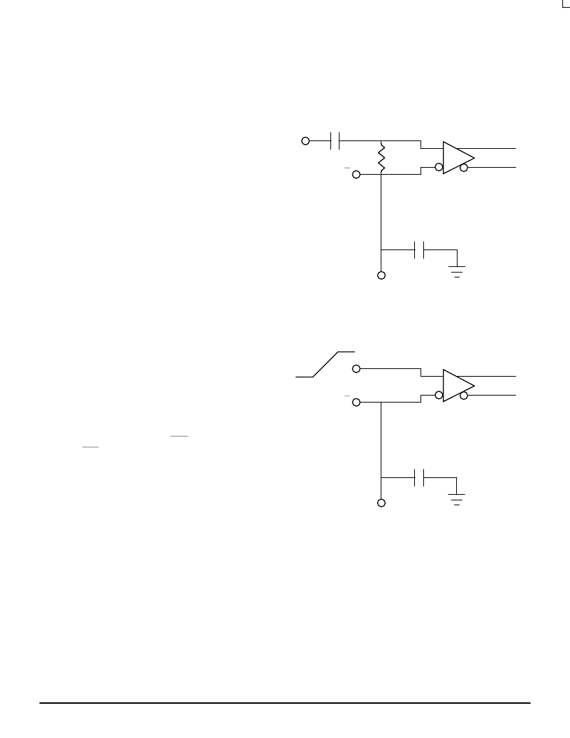
Differential versus Single-Ended Use
As can be seen from the data sheet, to minimize the skew
of the E211 the device must be used in the differential mode.
In the single-ended mode the propagation delays are
dependent on the relative position of the VBB switching
reference. Any VBB offset from the center of the input swing
will add delay to either the TPLH or TPHL and subtract delay
from the other. This increase and decrease in delay will lead
to an increase in the duty cycle skew and thus part-to-part
skew. The within-device skew will be independent of the VBB
and therefore will be the same regardless of whether the
device is driven differentially or single-endedly.
For applications where part-to-part skew or duty cycle
skew are not important the advantages of single-ended clock
distribution may lead to its use. Using single-ended
interconnect will reduce the number of signal traces to be
routed, but remember that all of the complimentary outputs
still need to be terminated therefore there will be no reduction
in the termination components required. To use the E211 with
a single-ended input the arrangement pictured in Figure 2b
should be used. If the input to the differential CLK inputs are
AC coupled as pictured in Figure 2a the dependence on a
centered VBB reference is removed. The situation pictured
will ensure that the input is centered around the bias set by
the VBB. As a result when AC coupled the AC specification
limits for a differential input can be used. For more
information on AC coupling please refer to the interfacing
section of the design guide in the ECLinPS data book.
Using the Enable Pins
Both the common enable (CEN) and the individual
enables (ENx) are synchronous to the CLK or SCLK input
depending on which is selected. The active low signals are
clocked into the enable flip flops on the negative edges of the
E211 clock inputs. In this way the devices will only be
disabled when the outputs are already in the LOW state. The
internal propagation delays are such that the delay to the
output through the distribution buffers is less than that
through the enable flip flops. This will ensure that the
disabling of the device will not slice any time off the clock
pulse. On initial power up the enable flip flops will randomly
attain a stable state, therefore precautions should be taken
on initial power up to ensure the E211 is in the desired state.
IN
IN
0.01
μ
F
VBB
50
0.001
μ
F
IN
0.01
μ
F
Figure 2a. AC Coupled Input
VBB
Figure 2b. Single-Ended Input
IN
相关PDF资料 |
PDF描述 |
|---|---|
| MC100EP111 | Low-Voltage 1:10 Differential ECL/PECL/HSTL Clock Driver(低压1:10差分ECL/PECL/HSTL时钟驱动器) |
| MC100H603FN | 9-Bit Latch ECL/TTL Translator |
| MC10H603 | 9-Bit Latch ECL/TTL Translator |
| MC10H603FN | 9-Bit Latch ECL/TTL Translator |
| MC100H642FN | 68030/040 PECL-TTL CLOCK DRIVER |
相关代理商/技术参数 |
参数描述 |
|---|---|
| MC10E211FNG | 功能描述:时钟驱动器及分配 5V ECL 1:6 Diff Clock Driver RoHS:否 制造商:Micrel 乘法/除法因子:1:4 输出类型:Differential 最大输出频率:4.2 GHz 电源电压-最大: 电源电压-最小:5 V 最大工作温度:+ 85 C 封装 / 箱体:SOIC-8 封装:Reel |
| MC10E211FNR2 | 功能描述:时钟驱动器及分配 5V ECL 1:6 Diff RoHS:否 制造商:Micrel 乘法/除法因子:1:4 输出类型:Differential 最大输出频率:4.2 GHz 电源电压-最大: 电源电压-最小:5 V 最大工作温度:+ 85 C 封装 / 箱体:SOIC-8 封装:Reel |
| MC10E211FNR2G | 功能描述:时钟驱动器及分配 5V ECL 1:6 Diff Clock Driver RoHS:否 制造商:Micrel 乘法/除法因子:1:4 输出类型:Differential 最大输出频率:4.2 GHz 电源电压-最大: 电源电压-最小:5 V 最大工作温度:+ 85 C 封装 / 箱体:SOIC-8 封装:Reel |
| MC10E212FN | 制造商:Rochester Electronics LLC 功能描述:- Bulk |
| MC10E212FNR2 | 制造商:Rochester Electronics LLC 功能描述:- Bulk |
发布紧急采购,3分钟左右您将得到回复。