参数资料
| 型号: | MC10EP29MNTXG |
| 厂商: | ON Semiconductor |
| 文件页数: | 1/10页 |
| 文件大小: | 0K |
| 描述: | IC FLIP FLOP DATA/CLK D 20-QFN |
| 标准包装: | 3,000 |
| 系列: | 10EP |
| 功能: | 设置(预设)和复位 |
| 类型: | D 型 |
| 输出类型: | 差分 |
| 元件数: | 2 |
| 每个元件的位元数: | 1 |
| 频率 - 时钟: | 3GHz |
| 延迟时间 - 传输: | 420ps |
| 触发器类型: | 正,负 |
| 电源电压: | 3 V ~ 5.5 V |
| 工作温度: | -40°C ~ 85°C |
| 安装类型: | 表面贴装 |
| 封装/外壳: | 20-VFQFN 裸露焊盘 |
| 包装: | 带卷 (TR) |
Semiconductor Components Industries, LLC, 2009
June, 2009 Rev. 8
1
Publication Order Number:
MC10EP29/D
MC10EP29, MC100EP29
3.3V / 5VECL Dual
Differential Data and Clock
D Flip-Flop With Set and
Reset
Description
The MC10/100EP29 is a dual masterslave flipflop. The device
features fully differential Data and Clock inputs as well as outputs.
The MC10/100EP29 is functionally equivalent to the
MC10/100EL29. Data enters the master latch when the clock is LOW
and transfers to the slave upon a positive transition on the clock input.
The differential inputs have special circuitry which ensures device
stability under open input conditions. When both differential inputs
are left open the D input will pull down to VEE and the D input will
bias around VCC/2. The outputs will go to a defined state, however the
state will be random based on how the flip flop powers up.
Both flip flops feature asynchronous, overriding Set and Reset
inputs. Note that the Set and Reset inputs cannot both be HIGH
simultaneously.
The VBB pin, an internally generated voltage supply, is available to
this device only. For single-ended input conditions, the unused
differential input is connected to VBB as a switching reference voltage.
VBB may also rebias AC coupled inputs. When used, decouple VBB
and VCC via a 0.01 mF capacitor and limit current sourcing or sinking
to 0.5 mA. When not used, VBB should be left open.
The 100 Series contains temperature compensation.
Features
Maximum Frequency > 3 GHz Typical
500 ps Typical Propagation Delays
PECL Mode Operating Range: VCC = 3.0 V to 5.5 V
with VEE = 0 V
NECL Mode Operating Range: VCC = 0 V
with VEE = 3.0 V to 5.5 V
Open Input Default State
Safety Clamp on Inputs
These are PbFree Devices
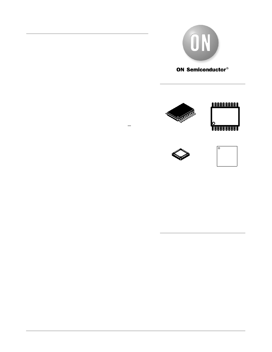
MARKING
DIAGRAM*
TSSOP20
DT SUFFIX
CASE 948E
XXXX
= MC10 or 100
A
= Assembly Location
L
= Wafer Lot
Y
= Year
W
= Work Week
G
= PbFree Package
*For additional marking information, refer to
Application Note AND8002/D.
http://onsemi.com
(Note: Microdot may be in either location)
See detailed ordering and shipping information in the package
dimensions section on page 8 of this data sheet.
ORDERING INFORMATION
XXXX
EP29
ALYWG
G
1
20
QFN20
MN SUFFIX
CASE 485E
XXXX
EP29
ALYWG
G
相关PDF资料 |
PDF描述 |
|---|---|
| RTD-2424/P-R | CONV DC/DC 2W 24VIN +/-24VOUT |
| MC100EP29MNTXG | IC FLIP FLOP DATA/CLK D 20-QFN |
| RTD-2424/P | CONV DC/DC 2W 24VIN +/-24VOUT |
| MC10EP29DTR2G | IC FLIP FLOP DUAL ECL DF 20TSSOP |
| RTD-2424/H-R | CONV DC/DC 2W 24VIN +/-24VOUT |
相关代理商/技术参数 |
参数描述 |
|---|---|
| MC10EP31D | 功能描述:触发器 3.3V/5V ECL D-Type RoHS:否 制造商:Texas Instruments 电路数量:2 逻辑系列:SN74 逻辑类型:D-Type Flip-Flop 极性:Inverting, Non-Inverting 输入类型:CMOS 输出类型: 传播延迟时间:4.4 ns 高电平输出电流:- 16 mA 低电平输出电流:16 mA 电源电压-最大:5.5 V 最大工作温度:+ 85 C 安装风格:SMD/SMT 封装 / 箱体:X2SON-8 封装:Reel |
| MC10EP31DG | 功能描述:触发器 3.3V/5V ECL D-Type w/Set and Reset RoHS:否 制造商:Texas Instruments 电路数量:2 逻辑系列:SN74 逻辑类型:D-Type Flip-Flop 极性:Inverting, Non-Inverting 输入类型:CMOS 输出类型: 传播延迟时间:4.4 ns 高电平输出电流:- 16 mA 低电平输出电流:16 mA 电源电压-最大:5.5 V 最大工作温度:+ 85 C 安装风格:SMD/SMT 封装 / 箱体:X2SON-8 封装:Reel |
| MC10EP31DR2 | 功能描述:触发器 3.3V/5V ECL D-Type RoHS:否 制造商:Texas Instruments 电路数量:2 逻辑系列:SN74 逻辑类型:D-Type Flip-Flop 极性:Inverting, Non-Inverting 输入类型:CMOS 输出类型: 传播延迟时间:4.4 ns 高电平输出电流:- 16 mA 低电平输出电流:16 mA 电源电压-最大:5.5 V 最大工作温度:+ 85 C 安装风格:SMD/SMT 封装 / 箱体:X2SON-8 封装:Reel |
| MC10EP31DR2G | 功能描述:触发器 3.3V/5V ECL D-Type w/Set and Reset RoHS:否 制造商:Texas Instruments 电路数量:2 逻辑系列:SN74 逻辑类型:D-Type Flip-Flop 极性:Inverting, Non-Inverting 输入类型:CMOS 输出类型: 传播延迟时间:4.4 ns 高电平输出电流:- 16 mA 低电平输出电流:16 mA 电源电压-最大:5.5 V 最大工作温度:+ 85 C 安装风格:SMD/SMT 封装 / 箱体:X2SON-8 封装:Reel |
| MC10EP31DT | 功能描述:触发器 3.3V/5V ECL D-Type RoHS:否 制造商:Texas Instruments 电路数量:2 逻辑系列:SN74 逻辑类型:D-Type Flip-Flop 极性:Inverting, Non-Inverting 输入类型:CMOS 输出类型: 传播延迟时间:4.4 ns 高电平输出电流:- 16 mA 低电平输出电流:16 mA 电源电压-最大:5.5 V 最大工作温度:+ 85 C 安装风格:SMD/SMT 封装 / 箱体:X2SON-8 封装:Reel |
发布紧急采购,3分钟左右您将得到回复。