参数资料
| 型号: | MC10H641FNG |
| 厂商: | ON Semiconductor |
| 文件页数: | 8/10页 |
| 文件大小: | 0K |
| 描述: | IC CLOCK BUFFER 1:9 65MHZ 28PLCC |
| 产品变化通告: | Dimensional change 21/Oct/2008 |
| 标准包装: | 37 |
| 类型: | 扇出缓冲器(分配) |
| 电路数: | 1 |
| 比率 - 输入:输出: | 1:9 |
| 差分 - 输入:输出: | 是/是 |
| 输入: | PECL |
| 输出: | TTL |
| 频率 - 最大: | 65MHz |
| 电源电压: | 4.75 V ~ 5.25 V |
| 工作温度: | 0°C ~ 85°C |
| 安装类型: | 表面贴装 |
| 封装/外壳: | 28-LCC(J 形引线) |
| 供应商设备封装: | 28-PLCC(11.51x11.51) |
| 包装: | 管件 |
MC10H641, MC100H641
http://onsemi.com
7
Rise/Fall Skew Determination
The risetofall skew is defined as simply the difference
between the TPLH and the TPHL propagation delays. This
skew for the H641 is dependent on the VCC applied to the
device. Notice from Figure 4 the opposite relationship of
TPD versus VCC between TPLH and TPHL. Because of this
the risetofall skew will vary depending on VCC. Since in
all likelihood it will be impossible to establish the exact
value for VCC, the expected variation range for VCC should
be used. If this variation will be the ± 5% shown in the data
sheet the risetofall skew could be established by simply
subtracting the fastest TPLH from the slowest TPHL; this
exercise yields 1.41 ns. If a tighter VCC range can be realized
Figure 4 can be used to establish the risetofall skew.
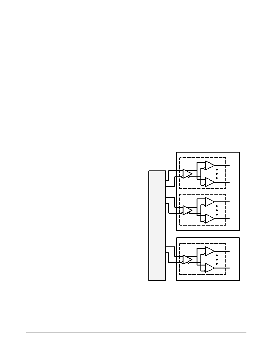
Specification Limit Determination Example
The situation pictured in Figure 6 will be analyzed as an
example. The central clock is distributed to two different
cards; on one card a single H641 is used to distribute the
clock while on the second card two H641’s are required to
supply the needed clocks. The data sheet as well as the
graphical information of this section will be used to
calculate the skew between H641a and H641b as well as the
skew between all three of the devices. Only the TPLH will be
analyzed, the TPHL numbers can be found using the same
technique. The following assumptions will be used:
All outputs will be loaded with 50 pF
All outputs will toggle at 30 MHz
The VCC variation between the two boards is ± 3 %
The temperature variation between the three
devices is ± 15°C around an ambient of 45°C.
500 lfpm air flow
The first task is to calculate the junction temperature for
the devices under these conditions. Using the power
equation yields:
PD =ICC (no load) * VCC +
VCC * VS * f * CL * # outputs
=4.3 * 48m A * 5.0 V + 5.0 V * 3.0 V * 30 MHz *
50 pF * 9
=432 mW + 203 mW = 635 mW
Using the thermal resistance graph of Figure 2 yields a
thermal resistance of 41°C/W which yields a junction
temperature of 71°C with a range of 56°C to 86°C. Using the
TPD versus Temperature curve of Figure 3 yields a
propagation delay of 5.42 ns and a variation of 0.19 ns.
Since the design will not experience the full ± 5% VCC
variation of the data sheet the 1.0 ns window provided will
be unnecessarily conservative. Using the curve of Figure 4
shows a delay variation due to a ± 3% VCC variation of
± 0.075 ns. Therefore the 1.0 ns window can be reduced to
1.0 ns (0.27 ns 0.15 ns) = 0.88 ns. Since H641a and
H641b are on the same board we will assume that they will
always be at the same VCC; therefore the propagation delay
window will only be 1 ns 0.27 ns = 0.73 ns.
Putting all of this information together leads to a skew
between all devices of
0.19 ns + 0.88 ns
(temperature + supply, and inherent device),
while the skew between devices A and B will be only
0.19 ns + 0.73 ns
(temperature + inherent device only).
In both cases, the propagation delays will be centered
around 5.42 ns, resulting in the following tPLH windows:
TPLH = 4.92 ns 5.99 ns; 1.07 ns window
(all devices)
TPLH= 5.00 ns 5.92 ns; 0.92 ns window
(devices a & b)
Of course the outputtooutput skew will be as shown in
the data sheet since all outputs are equally loaded.
This process may seem cumbersome, however the delay
windows, and thus skew, obtained are significantly better
than the conservative worst case limits provided at the
beginning of this note. For very high performance designs,
this extra information and effort can mean the difference
between going ahead with prototypes or spending valuable
engineering time searching for alternative approaches.
Q0
Q8
TTL
ECL
H641a
Q0
Q8
TTL
ECL
H641b
Q0
Q8
TTL
ECL
H641c
Card 1
Card 2
BACKPLANE
Figure 6. Example Application
相关PDF资料 |
PDF描述 |
|---|---|
| MC100H646FNG | IC CLK BUFFER 2:8 80MHZ 28-PLCC |
| NB7V33MMNG | IC CLOCK DIVIDER 1:1 10GHZ 16QFN |
| AD5453YUJZ-REEL7 | IC DAC 14BIT MULT 50MHZ TSOT23-8 |
| AD5308ARU | IC DAC 8BIT OCTAL W/BUFF 16TSSOP |
| MC100EP809FAG | IC CLOCK BUFFER MUX 1:9 32-LQFP |
相关代理商/技术参数 |
参数描述 |
|---|---|
| MC10H641FNR2 | 功能描述:转换 - 电压电平 5V PECL to TTL 1:9 RoHS:否 制造商:Micrel 类型:CML/LVDS/LVPECL to LVCMOS/LVTTL 传播延迟时间:1.9 ns 电源电流:14 mA 电源电压-最大:3.6 V 电源电压-最小:3 V 最大工作温度:+ 85 C 安装风格:SMD/SMT 封装 / 箱体:MLF-8 |
| MC10H641FNR2G | 功能描述:转换 - 电压电平 5V PECL to TTL 1:9 Clock Driver RoHS:否 制造商:Micrel 类型:CML/LVDS/LVPECL to LVCMOS/LVTTL 传播延迟时间:1.9 ns 电源电流:14 mA 电源电压-最大:3.6 V 电源电压-最小:3 V 最大工作温度:+ 85 C 安装风格:SMD/SMT 封装 / 箱体:MLF-8 |
| MC10H642 C57M WAF | 制造商:ON Semiconductor 功能描述: |
| MC10H642FN | 功能描述:时钟驱动器及分配 ECL/TTL Clock Driver RoHS:否 制造商:Micrel 乘法/除法因子:1:4 输出类型:Differential 最大输出频率:4.2 GHz 电源电压-最大: 电源电压-最小:5 V 最大工作温度:+ 85 C 封装 / 箱体:SOIC-8 封装:Reel |
| MC10H642FNG | 功能描述:时钟驱动器及分配 BBG ECL/TTL Clock Driver RoHS:否 制造商:Micrel 乘法/除法因子:1:4 输出类型:Differential 最大输出频率:4.2 GHz 电源电压-最大: 电源电压-最小:5 V 最大工作温度:+ 85 C 封装 / 箱体:SOIC-8 封装:Reel |
发布紧急采购,3分钟左右您将得到回复。