- 您现在的位置:买卖IC网 > PDF目录69024 > MC13226V (FREESCALE SEMICONDUCTOR INC) SPECIALTY MICROPROCESSOR CIRCUIT, PBGA99 PDF资料下载
参数资料
| 型号: | MC13226V |
| 厂商: | FREESCALE SEMICONDUCTOR INC |
| 元件分类: | 微控制器/微处理器 |
| 英文描述: | SPECIALTY MICROPROCESSOR CIRCUIT, PBGA99 |
| 封装: | 9.50 X 9.50 MM, 1.20 MM HEIGHT, ROHS COMPLIANT, LGA-99 |
| 文件页数: | 19/54页 |
| 文件大小: | 490K |
| 代理商: | MC13226V |
第1页第2页第3页第4页第5页第6页第7页第8页第9页第10页第11页第12页第13页第14页第15页第16页第17页第18页当前第19页第20页第21页第22页第23页第24页第25页第26页第27页第28页第29页第30页第31页第32页第33页第34页第35页第36页第37页第38页第39页第40页第41页第42页第43页第44页第45页第46页第47页第48页第49页第50页第51页第52页第53页第54页
MC1322x Technical Data, Rev. 1.3
26
Freescale Semiconductor
5.8
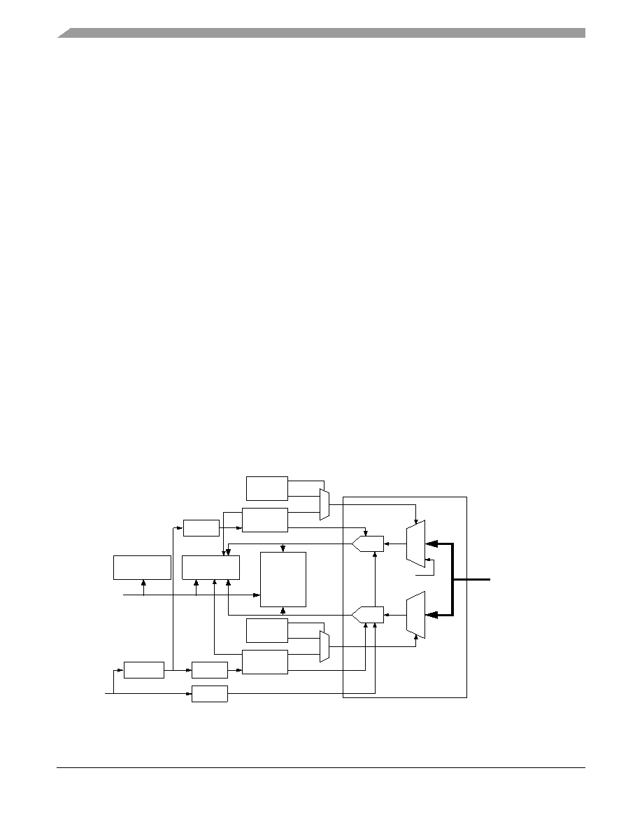
Analog-to-Digital Converter (ADC) Module
The MC1322x ADC module provides two 12-bit analog-to-digital converters (ADC_1 and ADC_2) with
eight external channels (ADC7 - ADC0) that can be multiplexed to either ADC. ADC_1 can also sample
a battery reference voltage for monitoring purposes. External pins (ADC2_VREFH, ADC2_VREFL,
ADC1_VREFH, and ADC1_VREFL) are provided for independent ADC reference voltages. The
minimum sample time is 20 s. Figure 8 shows a block diagram of the ADC module.
Each ADC can be programmed to scan multiple selected channels on a timed basis. The primary clock to
the ADC module is the peripheral reference clock (typically 24 MHz). For the time period between scan
sequences, the primary clock is first divided by an 8-bit prescale (1-255), and the derived clock drives both
the 32-bit delay timer and the ADC sequencer. Each ADC has its own delay timer and sequencer.
Once a scan sequence has been initiated, all selected channels can be sampled. Registers are provided to
define thresholds that can be enabled for the sampled channels. A threshold can be assigned to a specific
channel and can be programmed to be a less-than or greater-than threshold. Multiple thresholds can be
assigned to a single channel. Warm-up of the analog portion of the ADC circuitry is provided for power
management, and a separate 300 kHz ADC clock must be programmed via its own divider.
The battery monitor has two (2) dedicated threshold registers to set the high and low limits of the battery
sample channel.
Sample values are stored in a 8x16-bit FIFO. The FIFO accumulates samples from both ADCs, and the
12-bit sample value and a 4-bit channel tag are saved for each sample. The FIFO is read by the CPU from
a register address.
The module can be programmed to interrupt the processor based on the timed sample activity. Sample
activity, sequencer activity, or FIFO “fullness” can all be enabled to generate an interrupt.
The ADCs can also be overridden to sample on command as opposed to sequencer, time-based activity.
Figure 8. ADC Module Block Diagram
M
U
X
M
U
X
A n alog C h ann els
AD C 0 - ADC7
B a tte ry
ADC _1
ADC _2
FIF O
(8 x 16-B it,
12 -b it
va lu e + 4-
b it ch annel
Tag)
C ontro l
Reg is ters
Div id e r
M
U
X
Con tro l
O v errid e
Mo d e
Seq u en c er
2
M
U
X
Con tro l
O v errid e
Mo d e
Seq u en c er
1
Co m p a re
MC U
DAT A
BUS
P rescale r
An alo g
AD C2 M ux Se l
A DC1 M u x S el
AD C1 Ena ble
AD C 2 En ab le
AD
C
Cl
oc
k
A
D
C
Cl
o
c
k
32-B it
Tim e r
32-B it
Tim er
P eriph era l
R e fe rence C lock
300 kH z
相关PDF资料 |
PDF描述 |
|---|---|
| MC13226VR2 | SPECIALTY MICROPROCESSOR CIRCUIT, PBGA99 |
| MC13224V | SPECIALTY MICROPROCESSOR CIRCUIT, PBGA99 |
| MC141556P1 | UNIVERSAL SERIAL BUS CONTROLLER, PDIP28 |
| MC141556P1 | UNIVERSAL SERIAL BUS CONTROLLER, PDIP28 |
| MC14536BFL2 | 1 TIMER(S), PROGRAMMABLE TIMER, PDSO16 |
相关代理商/技术参数 |
参数描述 |
|---|---|
| MC13226VR2 | 功能描述:射频收发器 Kaibab PRO ROM SE 1.0 RoHS:否 制造商:Atmel 频率范围:2322 MHz to 2527 MHz 最大数据速率:2000 Kbps 调制格式:OQPSK 输出功率:4 dBm 类型: 工作电源电压:1.8 V to 3.6 V 最大工作温度:+ 85 C 接口类型:SPI 封装 / 箱体:QFN-32 封装:Tray |
| MC1322X | 制造商:FREESCALE 制造商全称:Freescale Semiconductor, Inc 功能描述:Advanced ZigBee?- Compliant Platform-in-Package (PiP) for the 2.4 GHz IEEE? 802.15.4 Standard |
| MC132333C | 制造商:FREESCALE 制造商全称:Freescale Semiconductor, Inc 功能描述:Low Cost SoC Remote Control Platform for the 2.4 GHz IEEE? 802.15.4 Standard |
| MC13233C | 功能描述:射频收发器 82KB FLASH 5KB RAM RoHS:否 制造商:Atmel 频率范围:2322 MHz to 2527 MHz 最大数据速率:2000 Kbps 调制格式:OQPSK 输出功率:4 dBm 类型: 工作电源电压:1.8 V to 3.6 V 最大工作温度:+ 85 C 接口类型:SPI 封装 / 箱体:QFN-32 封装:Tray |
| MC13233CR2 | 功能描述:射频收发器 82KB FLASH 5KB RAM RoHS:否 制造商:Atmel 频率范围:2322 MHz to 2527 MHz 最大数据速率:2000 Kbps 调制格式:OQPSK 输出功率:4 dBm 类型: 工作电源电压:1.8 V to 3.6 V 最大工作温度:+ 85 C 接口类型:SPI 封装 / 箱体:QFN-32 封装:Tray |
发布紧急采购,3分钟左右您将得到回复。