- 您现在的位置:买卖IC网 > PDF目录26795 > MC14013BFR2 (ON SEMICONDUCTOR) 4000/14000/40000 SERIES, DUAL POSITIVE EDGE TRIGGERED D FLIP-FLOP, COMPLEMENTARY OUTPUT, PDSO14 PDF资料下载
参数资料
| 型号: | MC14013BFR2 |
| 厂商: | ON SEMICONDUCTOR |
| 元件分类: | 锁存器 |
| 英文描述: | 4000/14000/40000 SERIES, DUAL POSITIVE EDGE TRIGGERED D FLIP-FLOP, COMPLEMENTARY OUTPUT, PDSO14 |
| 封装: | EIAJ, SO-14 |
| 文件页数: | 1/9页 |
| 文件大小: | 162K |
| 代理商: | MC14013BFR2 |
Semiconductor Components Industries, LLC, 2006
October, 2006 Rev. 7
1
Publication Order Number:
MC14013B/D
MC14013B
Dual Type D FlipFlop
The MC14013B dual type D flipflop is constructed with MOS
Pchannel and Nchannel enhancement mode devices in a single
monolithic structure. Each flipflop has independent Data, (D), Direct
Set, (S), Direct Reset, (R), and Clock (C) inputs and complementary
outputs (Q and Q). These devices may be used as shift register
elements or as type T flipflops for counter and toggle applications.
Features
Static Operation
Diode Protection on All Inputs
Supply Voltage Range = 3.0 Vdc to 18 Vdc
Logic EdgeClocked FlipFlop Design
Logic state is retained indefinitely with clock level either high or
low; information is transferred to the output only on the
positivegoing edge of the clock pulse
Capable of Driving Two Lowpower TTL Loads or One Lowpower
Schottky TTL Load Over the Rated Temperature Range
PinforPin Replacement for CD4013B
PbFree Packages are Available
MAXIMUM RATINGS (Voltages Referenced to VSS)
Symbol
Parameter
Value
Unit
VDD
DC Supply Voltage Range
0.5 to +18.0
V
Vin, Vout Input or Output Voltage Range
(DC or Transient)
0.5 to VDD + 0.5
V
Iin, Iout
Input or Output Current
(DC or Transient) per Pin
± 10
mA
PD
Power Dissipation, per Package
(Note 1)
500
mW
TA
Ambient Temperature Range
55 to +125
°C
Tstg
Storage Temperature Range
65 to +150
°C
TL
Lead Temperature
(8Second Soldering)
260
°C
Stresses exceeding Maximum Ratings may damage the device. Maximum
Ratings are stress ratings only. Functional operation above the Recommended
Operating Conditions is not implied. Extended exposure to stresses above the
Recommended Operating Conditions may affect device reliability.
1. Temperature Derating:
Plastic “P and D/DW” Packages: – 7.0 mW/_C From 65_C To 125_C
This device contains protection circuitry to guard against damage due to high
static voltages or electric fields. However, precautions must be taken to avoid
applications of any voltage higher than maximum rated voltages to this
highimpedance circuit. For proper operation, Vin and Vout should be constrained
to the range VSS v (Vin or Vout) v VDD.
Unused inputs must always be tied to an appropriate logic voltage level
(e.g., either VSS or VDD). Unused outputs must be left open.
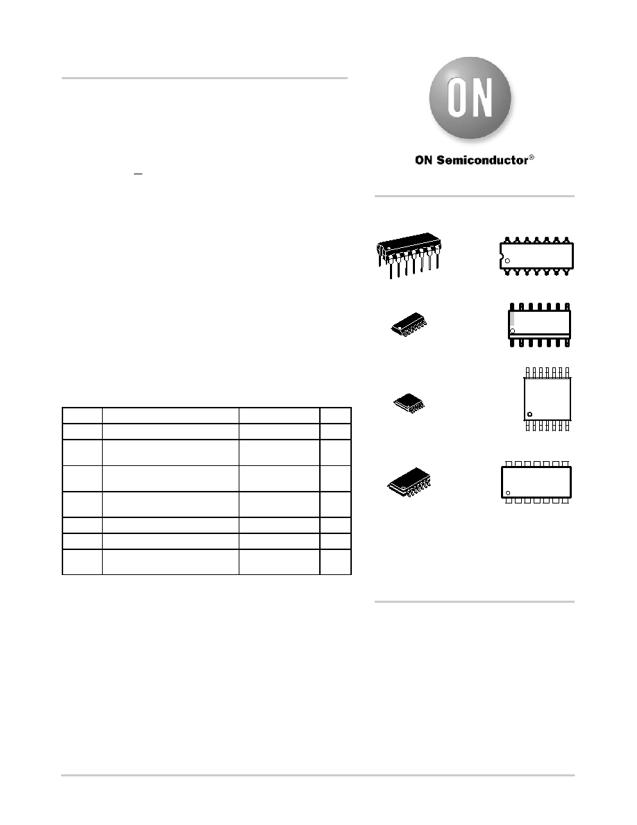
MARKING
DIAGRAMS
1
14
PDIP14
P SUFFIX
CASE 646
MC14013BCP
AWLYYWWG
SOIC14
D SUFFIX
CASE 751A
TSSOP14
DT SUFFIX
CASE 948G
1
14
14013BG
AWLYWW
14
013B
ALYW G
G
1
14
A
= Assembly Location
WL, L
= Wafer Lot
YY, Y
= Year
WW, W = Work Week
G or G
= PbFree Package
SOEIAJ14
F SUFFIX
CASE 965
1
14
MC14013B
ALYWG
See detailed ordering and shipping information in the package
dimensions section on page 2 of this data sheet.
ORDERING INFORMATION
http://onsemi.com
(Note: Microdot may be in either location)
相关PDF资料 |
PDF描述 |
|---|---|
| MC14014BD | 4000/14000/40000 SERIES, 8-BIT RIGHT PARALLEL IN SERIAL OUT SHIFT REGISTER, TRUE OUTPUT, PDSO16 |
| MC14015BCPDS | 4000/14000/40000 SERIES, 4-BIT RIGHT SERIAL IN PARALLEL OUT SHIFT REGISTER, TRUE OUTPUT, PDIP16 |
| MC14015BALD | 4000/14000/40000 SERIES, 4-BIT RIGHT SERIAL IN PARALLEL OUT SHIFT REGISTER, TRUE OUTPUT, CDIP16 |
| MC14017BAL | 4000/14000/40000 SERIES, SYN POSITIVE EDGE TRIGGERED 10-BIT UP RING COUNTER, CDIP16 |
| MC14017BCLD | 4000/14000/40000 SERIES, SYN POSITIVE EDGE TRIGGERED 10-BIT UP RING COUNTER, CDIP16 |
相关代理商/技术参数 |
参数描述 |
|---|---|
| MC14014B | 制造商:ONSEMI 制造商全称:ON Semiconductor 功能描述:8-Bit Static Shift Register |
| MC14014BCL | 制造商:Rochester Electronics LLC 功能描述:- Bulk |
| MC14014BCP | 功能描述:计数器移位寄存器 3-18V 8-Bit CMOS RoHS:否 制造商:Texas Instruments 计数器类型: 计数顺序:Serial to Serial/Parallel 电路数量:1 封装 / 箱体:SOIC-20 Wide 逻辑系列: 逻辑类型: 输入线路数量:1 输出类型:Open Drain 传播延迟时间:650 ns 最大工作温度:+ 125 C 最小工作温度:- 40 C 封装:Reel |
| MC14014BCPD | 制造商:Motorola Inc 功能描述: |
| MC14014BCPG | 功能描述:计数器移位寄存器 3-18V 8-Bit CMOS Static Shift RoHS:否 制造商:Texas Instruments 计数器类型: 计数顺序:Serial to Serial/Parallel 电路数量:1 封装 / 箱体:SOIC-20 Wide 逻辑系列: 逻辑类型: 输入线路数量:1 输出类型:Open Drain 传播延迟时间:650 ns 最大工作温度:+ 125 C 最小工作温度:- 40 C 封装:Reel |
发布紧急采购,3分钟左右您将得到回复。