参数资料
| 型号: | MC14027BDR2G |
| 厂商: | ON Semiconductor |
| 文件页数: | 1/7页 |
| 文件大小: | 0K |
| 描述: | IC FLIP FLOP JK DUAL CMOS 16SOIC |
| 标准包装: | 1 |
| 系列: | 4000B |
| 功能: | 设置(预设)和复位 |
| 类型: | JK 型 |
| 输出类型: | 差分 |
| 元件数: | 2 |
| 每个元件的位元数: | 1 |
| 频率 - 时钟: | 13MHz |
| 延迟时间 - 传输: | 50ns |
| 触发器类型: | 正边沿 |
| 输出电流高,低: | 8.8mA,8.8mA |
| 电源电压: | 3 V ~ 18 V |
| 工作温度: | -55°C ~ 125°C |
| 安装类型: | 表面贴装 |
| 封装/外壳: | 16-SOIC(0.154",3.90mm 宽) |
| 包装: | 标准包装 |
| 其它名称: | MC14027BDR2GOSDKR |
Semiconductor Components Industries, LLC, 2013
April, 2013 Rev. 7
1
Publication Order Number:
MC14027B/D
MC14027B
Dual J-K Flip-Flop
The MC14027B dual JK flipflop has independent J, K, Clock (C),
Set (S) and Reset (R) inputs for each flipflop. These devices may be
used in control, register, or toggle functions.
Features
Diode Protection on All Inputs
Supply Voltage Range = 3.0 Vdc to 18 Vdc
Logic Swing Independent of Fanout
Logic EdgeClocked FlipFlop Design
Logic State is Retained Indefinitely with Clock Level Either High or
Low; Information is Transferred to the Output Only on the
PositiveGoing Edge of the Clock Pulse
Capable of Driving Two LowPower TTL Loads or One LowPower
Schottky TTL Load Over the Rated Temperature Range
PinforPin Replacement for CD4027B
These Devices are PbFree and are RoHS Compliant
NLV Prefix for Automotive and Other Applications Requiring
Unique Site and Control Change Requirements; AECQ100
Qualified and PPAP Capable
MAXIMUM RATINGS (Voltages Referenced to VSS)
Symbol
Parameter
Value
Unit
VDD
DC Supply Voltage Range
0.5 to +18.0
V
Vin, Vout
Input or Output Voltage Range
(DC or Transient)
0.5 to VDD + 0.5
V
Iin, Iout
Input or Output Current
(DC or Transient) per Pin
±10
mA
PD
Power Dissipation, per Package
(Note 1)
500
mW
TA
Ambient Temperature Range
55 to +125
°C
Tstg
Storage Temperature Range
65 to +150
°C
TL
Lead Temperature
(8Second Soldering)
260
°C
Stresses exceeding Maximum Ratings may damage the device. Maximum
Ratings are stress ratings only. Functional operation above the Recommended
Operating Conditions is not implied. Extended exposure to stresses above the
Recommended Operating Conditions may affect device reliability.
1. Temperature Derating:
Plastic “P and D/DW” Packages: – 7.0 mW/_C From 65_C To 125_C
This device contains protection circuitry to guard against damage due to high
static voltages or electric fields. However, precautions must be taken to avoid
applications of any voltage higher than maximum rated voltages to this
highimpedance circuit. For proper operation, Vin and Vout should be constrained
to the range VSS v (Vin or Vout) v VDD.
Unused inputs must always be tied to an appropriate logic voltage level (e.g.,
either VSS or VDD). Unused outputs must be left open.
http://onsemi.com
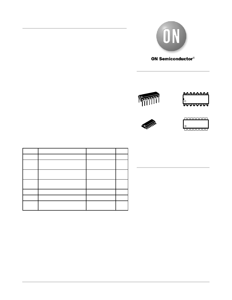
MARKING
DIAGRAMS
PDIP16
P SUFFIX
CASE 648
MC14027BCP
AWLYYWWG
SOIC16
D SUFFIX
CASE 751B
14027BG
AWLYWW
A
= Assembly Location
WL
= Wafer Lot
YY, Y
= Year
WW
= Work Week
G
= PbFree Indicator
See detailed ordering and shipping information in the package
dimensions section on page 3 of this data sheet.
ORDERING INFORMATION
16
1
16
相关PDF资料 |
PDF描述 |
|---|---|
| M85049/26-2-18 | CRIMP RING SHELL SIZE 18 |
| M85049/31-22W-SKI | E NUT SHELL SIZE 22 CADMIUM |
| MM74HC74AMTCX | IC FLIP FLOP DUAL D 14TSSOP |
| 74LVX74MTCX | IC FLIP FLOP DUAL DTYPE 14TSSOP |
| M85049/52-1-14N | STRAIN RLF .875-20 UNEF NICKEL |
相关代理商/技术参数 |
参数描述 |
|---|---|
| MC14027BF | 制造商:Rochester Electronics LLC 功能描述:- Bulk |
| MC14027BFEL | 功能描述:触发器 3-18V CMOS Dual RoHS:否 制造商:Texas Instruments 电路数量:2 逻辑系列:SN74 逻辑类型:D-Type Flip-Flop 极性:Inverting, Non-Inverting 输入类型:CMOS 输出类型: 传播延迟时间:4.4 ns 高电平输出电流:- 16 mA 低电平输出电流:16 mA 电源电压-最大:5.5 V 最大工作温度:+ 85 C 安装风格:SMD/SMT 封装 / 箱体:X2SON-8 封装:Reel |
| MC14027BFELG | 功能描述:触发器 3-18V CMOS Dual JK-Type RoHS:否 制造商:Texas Instruments 电路数量:2 逻辑系列:SN74 逻辑类型:D-Type Flip-Flop 极性:Inverting, Non-Inverting 输入类型:CMOS 输出类型: 传播延迟时间:4.4 ns 高电平输出电流:- 16 mA 低电平输出电流:16 mA 电源电压-最大:5.5 V 最大工作温度:+ 85 C 安装风格:SMD/SMT 封装 / 箱体:X2SON-8 封装:Reel |
| MC14027BFL1 | 制造商:Rochester Electronics LLC 功能描述:- Bulk |
| MC14027BFR1 | 制造商:Rochester Electronics LLC 功能描述:- Bulk |
发布紧急采购,3分钟左右您将得到回复。