- 您现在的位置:买卖IC网 > PDF目录26797 > MC14073BFR1 (ON SEMICONDUCTOR) 4000/14000/40000 SERIES, TRIPLE 3-INPUT AND GATE, PDSO14 PDF资料下载
参数资料
| 型号: | MC14073BFR1 |
| 厂商: | ON SEMICONDUCTOR |
| 元件分类: | 门电路 |
| 英文描述: | 4000/14000/40000 SERIES, TRIPLE 3-INPUT AND GATE, PDSO14 |
| 封装: | EIAJ, PLASTIC, SOIC-14 |
| 文件页数: | 1/21页 |
| 文件大小: | 255K |
| 代理商: | MC14073BFR1 |
Semiconductor Components Industries, LLC, 2000
August, 2000 – Rev. 2
1
Publication Order Number:
MC14001B/D
MC14001B Series
B-Suffix Series CMOS Gates
MC14001B, MC14011B, MC14023B,
MC14025B, MC14071B, MC14073B,
MC14081B, MC14082B
The B Series logic gates are constructed with P and N channel
enhancement mode devices in a single monolithic structure
(Complementary MOS). Their primary use is where low power
dissipation and/or high noise immunity is desired.
Supply Voltage Range = 3.0 Vdc to 18 Vdc
All Outputs Buffered
Capable of Driving Two Low–power TTL Loads or One Low–power
Schottky TTL Load Over the Rated Temperature Range.
Double Diode Protection on All Inputs Except: Triple Diode
Protection on MC14011B and MC14081B
Pin–for–Pin Replacements for Corresponding CD4000 Series B
Suffix Devices
MAXIMUM RATINGS (Voltages Referenced to VSS) (Note 1.)
Symbol
Parameter
Value
Unit
VDD
DC Supply Voltage Range
–0.5 to +18.0
V
Vin, Vout
Input or Output Voltage Range
(DC or Transient)
–0.5 to VDD + 0.5
V
Iin, Iout
Input or Output Current
(DC or Transient) per Pin
±10
mA
PD
Power Dissipation,
per Package (Note 2.)
500
mW
TA
Ambient Temperature Range
–55 to +125
°C
Tstg
Storage Temperature Range
–65 to +150
°C
TL
Lead Temperature
(8–Second Soldering)
260
°C
1. Maximum Ratings are those values beyond which damage to the device
may occur.
2. Temperature Derating:
Plastic “P and D/DW” Packages: – 7.0 mW/
_C From 65_C To 125_C
This device contains protection circuitry to guard against damage due to high
static voltages or electric fields. However, precautions must be taken to avoid
applications of any voltage higher than maximum rated voltages to this
high–impedance circuit. For proper operation, Vin and Vout should be constrained
to the range VSS v (Vin or Vout) v VDD.
Unused inputs must always be tied to an appropriate logic voltage level (e.g.,
either VSS or VDD). Unused outputs must be left open.
http://onsemi.com
Device
Description
DEVICE INFORMATION
MC14001B
Quad 2–Input NOR Gate
MC14011B
Quad 2–Input NAND Gate
MC14023B
Triple 3–Input NAND Gate
MC14025B
Triple 3–Input NOR Gate
MC14071B
Quad 2–Input OR Gate
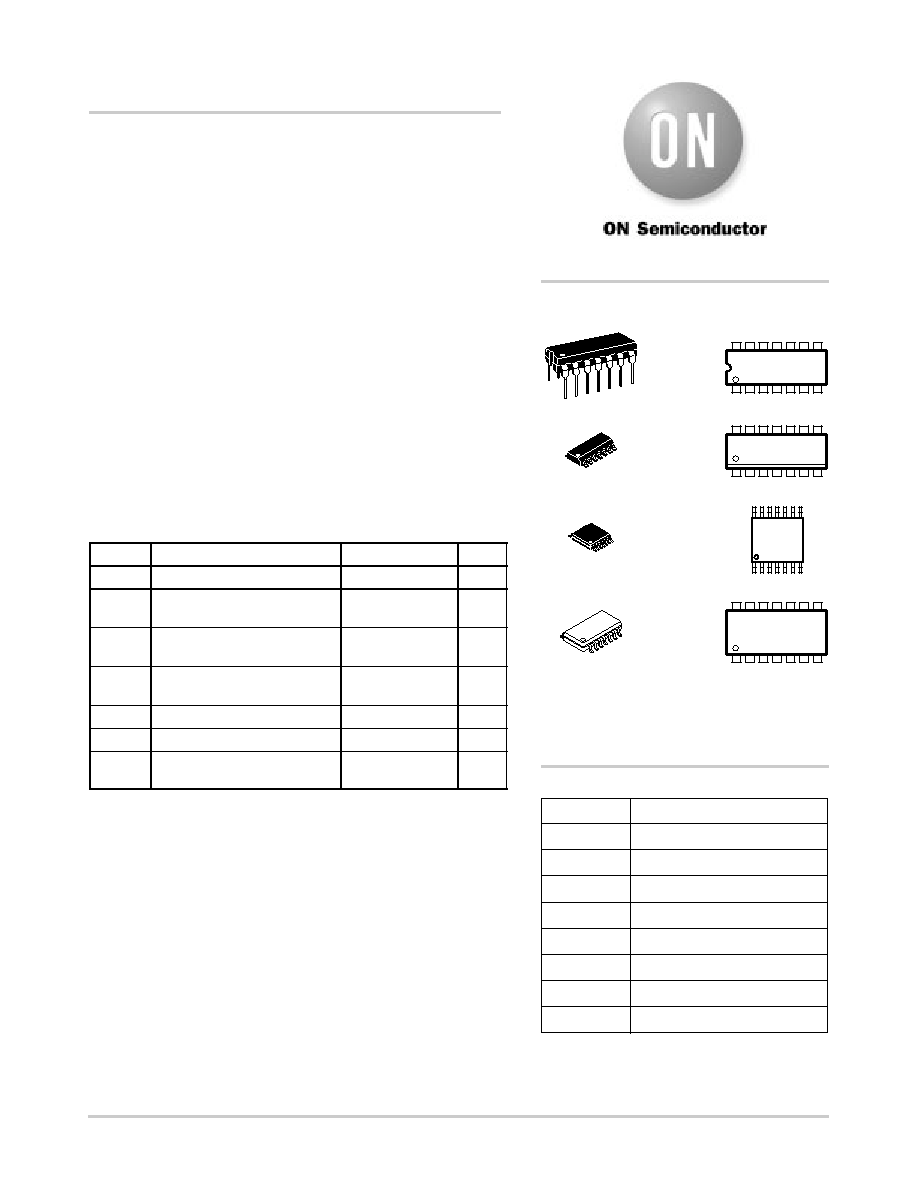
MARKING
DIAGRAMS
1
14
PDIP–14
P SUFFIX
CASE 646
MC140xxBCP
AWLYYWW
SOIC–14
D SUFFIX
CASE 751A
TSSOP–14
DT SUFFIX
CASE 948G
1
14
140xxB
AWLYWW
14
0xxB
ALYW
1
14
xx
= Specific Device Code
A
= Assembly Location
WL, L
= Wafer Lot
YY, Y
= Year
WW, W
= Work Week
SOEIAJ–14
F SUFFIX
CASE 965
1
14
MC140xxB
ALYW
MC14073B
Triple 3–Input AND Gate
MC14081B
Quad 2–Input AND Gate
MC14082B
Dual 4–Input AND Gate
See detailed ordering and shipping information in the package
dimensions section on page 11 of this data sheet.
ORDERING INFORMATION
相关PDF资料 |
PDF描述 |
|---|---|
| MC14081BFR1 | 4000/14000/40000 SERIES, QUAD 2-INPUT AND GATE, PDSO14 |
| MC14081BFL1 | 4000/14000/40000 SERIES, QUAD 2-INPUT AND GATE, PDSO14 |
| MC14071BFR2 | 4000/14000/40000 SERIES, QUAD 2-INPUT OR GATE, PDSO14 |
| MC14093BCPD | 4000/14000/40000 SERIES, QUAD 2-INPUT NAND GATE, PDIP14 |
| MC14093BDR2 | 4000/14000/40000 SERIES, QUAD 2-INPUT NAND GATE, PDSO14 |
相关代理商/技术参数 |
参数描述 |
|---|---|
| MC14075B | 制造商:Motorola Inc 功能描述: |
| MC14075BCL | 制造商:MOTOROLA 制造商全称:Motorola, Inc 功能描述:B-Suffix Series CMOS Gates |
| MC14075BCP | 制造商:Motorola Inc 功能描述: |
| MC14075BD | 制造商:MOTOROLA 制造商全称:Motorola, Inc 功能描述:B-Suffix Series CMOS Gates |
| MC14075BFEL | 制造商:Rochester Electronics LLC 功能描述:- Bulk |
发布紧急采购,3分钟左右您将得到回复。