- 您现在的位置:买卖IC网 > PDF目录29121 > MC14099BFL1 (ON SEMICONDUCTOR) 4000/14000/40000 SERIES, LOW LEVEL TRIGGERED D LATCH, TRUE OUTPUT, PDSO16 PDF资料下载
参数资料
| 型号: | MC14099BFL1 |
| 厂商: | ON SEMICONDUCTOR |
| 元件分类: | 锁存器 |
| 英文描述: | 4000/14000/40000 SERIES, LOW LEVEL TRIGGERED D LATCH, TRUE OUTPUT, PDSO16 |
| 封装: | EIAJ, PLASTIC, SOIC-16 |
| 文件页数: | 1/10页 |
| 文件大小: | 217K |
| 代理商: | MC14099BFL1 |
Semiconductor Components Industries, LLC, 2000
March, 2000 – Rev. 3
1
Publication Order Number:
MC14099B/D
MC14099B
8-Bit Addressable Latches
The MC14099B is an 8–bit addressable latch. Data is entered in
serial form when the appropriate latch is addressed (via address pins
A0, A1, A2) and write disable is in the low state. For the MC14099B
the input is a unidirectional write only port.
The data is presented in parallel at the output of the eight latches
independently of the state of Write Disable, Write/Read or Chip
Enable.
A Master Reset capability is available on both parts.
Serial Data Input
Parallel Output
Master Reset
Supply Voltage Range = 3.0 Vdc to 18 Vdc
Capable of Driving Two Low–power TTL Loads or One Low–Power
Schottky TTL Load over the Rated Temperature Range
MC14099B pin for pin compatible with CD4099B
MAXIMUM RATINGS (Voltages Referenced to VSS) (Note 2.)
Symbol
Parameter
Value
Unit
VDD
DC Supply Voltage Range
– 0.5 to +18.0
V
Vin, Vout
Input or Output Voltage Range
(DC or Transient)
– 0.5 to VDD + 0.5
V
Iin, Iout
Input or Output Current
(DC or Transient) per Pin
±10
mA
PD
Power Dissipation,
per Package (Note 3.)
500
mW
TA
Ambient Temperature Range
– 55 to +125
°C
Tstg
Storage Temperature Range
– 65 to +150
°C
TL
Lead Temperature
(8–Second Soldering)
260
°C
2. Maximum Ratings are those values beyond which damage to the device
may occur.
3. Temperature Derating:
Plastic “P and D/DW” Packages: – 7.0 mW/
_C From 65_C To 125_C
This device contains protection circuitry to guard against damage due to high
static voltages or electric fields. However, precautions must be taken to avoid
applications of any voltage higher than maximum rated voltages to this
high–impedance circuit. For proper operation, Vin and Vout should be constrained
to the range VSS v (Vin or Vout) v VDD.
Unused inputs must always be tied to an appropriate logic voltage level (e.g.,
either VSS or VDD). Unused outputs must be left open.
Device
Package
Shipping
ORDERING INFORMATION
MC14099BCP
PDIP–16
2000/Box
MC14099BDW
SOIC–16
http://onsemi.com
2350/Box
MC14099BDWR2
SOIC–16
1000/Tape & Reel
MC14099BF
SOEIAJ–16
See Note 1.
MC14099BFEL
SOEIAJ–16
See Note 1.
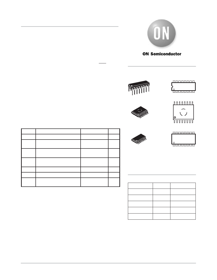
MARKING
DIAGRAMS
1
16
PDIP–16
P SUFFIX
CASE 648
MC14099BCP
AWLYYWW
A
= Assembly Location
WL or L
= Wafer Lot
YY or Y
= Year
WW or W = Work Week
SOEIAJ–16
F SUFFIX
CASE 966
1
16
MC14099B
AWLYWW
1. For ordering information on the EIAJ version of
the SOIC packages, please contact your local
ON Semiconductor representative.
SOIC–16
DW SUFFIX
CASE 751G
1
16
14099B
AWLYYWW
相关PDF资料 |
PDF描述 |
|---|---|
| MC14163BCP | 4000/14000/40000 SERIES, SYN POSITIVE EDGE TRIGGERED 4-BIT UP BINARY COUNTER, PDIP16 |
| MC14161BCL | 4000/14000/40000 SERIES, SYN POSITIVE EDGE TRIGGERED 4-BIT UP BINARY COUNTER, CDIP16 |
| MC14160BDR2 | 4000/14000/40000 SERIES, SYN POSITIVE EDGE TRIGGERED 4-BIT UP DECADE COUNTER, PDSO16 |
| MC14161BCPD | 4000/14000/40000 SERIES, SYN POSITIVE EDGE TRIGGERED 4-BIT UP BINARY COUNTER, PDIP16 |
| MC14162BCP | 4000/14000/40000 SERIES, SYN POSITIVE EDGE TRIGGERED 4-BIT UP DECADE COUNTER, PDIP16 |
相关代理商/技术参数 |
参数描述 |
|---|---|
| MC140B-6F | 制造商:SIG 功能描述: |
| MC-140P | 制造商:Panasonic Industrial Company 功能描述:BAG |
| MC141001BCP | 制造商:Motorola Inc 功能描述: |
| MC14106BCP | 功能描述:变换器 3-18V CMOS Hex RoHS:否 制造商:NXP Semiconductors 电路数量:6 逻辑系列:74ABT 逻辑类型:BiCMOS 高电平输出电流:- 15 mA 低电平输出电流:20 mA 传播延迟时间:2.2 ns 电源电压-最大:5.5 V 电源电压-最小:4.5 V 最大工作温度:+ 85 C 最小工作温度:- 40 C 工作温度范围: 封装 / 箱体:DIP-14 封装:Tube |
| MC14106BCPG | 功能描述:变换器 3-18V CMOS Hex Schmitt Trigger RoHS:否 制造商:NXP Semiconductors 电路数量:6 逻辑系列:74ABT 逻辑类型:BiCMOS 高电平输出电流:- 15 mA 低电平输出电流:20 mA 传播延迟时间:2.2 ns 电源电压-最大:5.5 V 电源电压-最小:4.5 V 最大工作温度:+ 85 C 最小工作温度:- 40 C 工作温度范围: 封装 / 箱体:DIP-14 封装:Tube |
发布紧急采购,3分钟左右您将得到回复。