- 您现在的位置:买卖IC网 > PDF目录20240 > MC14489BPE (Freescale Semiconductor)IC LED DRIVER 5-CH CMOS 20-DIP PDF资料下载
参数资料
| 型号: | MC14489BPE |
| 厂商: | Freescale Semiconductor |
| 文件页数: | 4/22页 |
| 文件大小: | 0K |
| 描述: | IC LED DRIVER 5-CH CMOS 20-DIP |
| 标准包装: | 18 |
| 显示器类型: | LED |
| 配置: | 7 段显示 |
| 接口: | 串行 |
| 电流 - 电源: | 5.5mA |
| 电源电压: | 4.5 V ~ 5.5 V |
| 工作温度: | -40°C ~ 130°C |
| 安装类型: | 通孔 |
| 封装/外壳: | 20-DIP(0.300",7.62mm) |
| 供应商设备封装: | 20-PDIP |
| 包装: | 管件 |
| 产品目录页面: | 809 (CN2011-ZH PDF) |
�� �
�
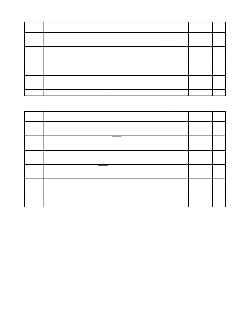
�AC� ELECTRICAL� CHARACTERISTICS� (TJ� =� –� 40� °� to� 130� °� C*,� CL� =� 50� pF,� Input� tr� =� tf� =� 10� ns)�
�VDD�
�Guaranteed�
�Symbol�
�fclk�
�tPLH,�
�tPHL�
�Parameter�
�Serial� Data� Clock� Frequency,� Single� Device� or� Cascaded� Devices�
�NOTE:� Refer� to� Clock� tw� below�
�(Figure� 1)�
�Maximum� Propagation� Delay,� Clock� to� Data� Out�
�(Figures� 1� and� 5)�
�V�
�3.0�
�4.5�
�5.5�
�3.0�
�4.5�
�Limit�
�dc� to� 3.0�
�dc� to� 4.0�
�dc� to� 4.0�
�140�
�80�
�Unit�
�MHz�
�ns�
�5.5�
�80�
�tTLH,�
�tTHL�
�Maximum� Output� Transistion� Time,� Data� Out�
�(Figures� 1� and� 5)�
�3.0�
�4.5�
�70�
�50�
�ns�
�5.5�
�50�
�fR�
�Refresh� Rate� —� Bank� 1� through� Bank� 5�
�(Figures� 2� and� 6)�
�3.0�
�4.5�
�NA�
�700� to� 1900�
�Hz�
�5.5�
�700� to� 1900�
�Cin�
�Maximum� Input� Capacitance� —� Data� In,� Clock,� Enable�
�—�
�10�
�pF�
�*� See� Thermal� Considerations� section.�
�TIMING� REQUIREMENTS� (TJ� =� –� 40� °� to� 130� °� C*,� Input� tr� =� tf� =� 10� ns� unless� otherwise� indicated� )�
�VDD�
�Guaranteed�
�Symbol�
�tsu,� th�
�Parameter�
�Minimum� Setup� and� Hold� Times,� Data� In� versus� Clock�
�(Figure� 3)�
�V�
�3.0�
�4.5�
�Limit�
�50�
�40�
�Unit�
�ns�
�5.5�
�40�
�tsu,� th,�
�trec�
�Minimum� Setup,� Hold,� **� and� Recovery� Times,� Enable� versus� Clock�
�(Figure� 4)�
�3.0�
�4.5�
�150�
�100�
�ns�
�5.5�
�100�
�tw(L)�
�Minimum� Active–Low� Pulse� Width,� Enable�
�(Figure� 4)�
�3.0�
�4.5�
�4.5�
�3.4�
�μ� s�
�5.5�
�3.4�
�tw(H)�
�Minimum� Inactive–High� Pulse� Width,� Enable�
�(Figure� 4)�
�3.0�
�4.5�
�300�
�150�
�ns�
�5.5�
�150�
�tw�
�Minimum� Pulse� Width,� Clock�
�(Figure� 1)�
�3.0�
�4.5�
�167�
�125�
�ns�
�5.5�
�125�
�tr,� tf�
�Maximum� Input� Rise� and� Fall� Times� —� Data� In,� Clock,� Enable�
�(Figure� 1)�
�3.0�
�4.5�
�1�
�1�
�ms�
�5.5�
�1�
�VDD� =� 4.5� to� 5.5� V,� clk� >� 2.34� MHz:� th� =� 3300� –� (7500/fclk)�
�*� See� Thermal� Considerations� section.�
�**� For� a� high–speed� 8–Clock� access,� th� for� Enable� is� determined� as� follows:�
�VDD� =� 3� to� 4.5� V,� fclk� >� 1.78� MHz:� th� =� 4350� –� (7500/fclk)�
�f�
�where� th� is� in� ns� and� fclk� is� in� MHz.�
�NOTES:�
�1.� This� restriction� does� NOT� apply� for� fclk� rates� less� than� those� listed� above.� For� “slow”� fclk� rates,� use� the� th� limits� in� the� above� table.�
�2.� This� restriction� does� NOT� apply� for� an� access� involving� more� than� 8� Clocks.� For� >� 8� Clocks,� use� the� th� limits� in� the� above� table.�
�MC14489B�
�4�
�MOTOROLA�
�相关PDF资料 |
PDF描述 |
|---|---|
| 202S48W103KV4E | CAP CER 10000PF 2KV 10% X7R 2225 |
| SRP7030-1R1FM | INDUCTOR POWER 1.1UH SHIELD SMD |
| SRP7030-R47FM | INDUCTOR POWER 0.47UH SHIELD SMD |
| RCB92DHRT-S378 | EDGECARD EXT PCI64 184PS .050 5V |
| T95R337K016HSSS | CAP TANT 330UF 16V 10% 2824 |
相关代理商/技术参数 |
参数描述 |
|---|---|
| MC14489P | 制造商:Motorola Inc 功能描述: |
| MC14490DW | 功能描述:算数逻辑单元 - ALU LOG CMOS 3-18V HEX BOUNCE ELIMINATOR RoHS:否 制造商:ON Semiconductor 高电平输出电流: 低电平输出电流: 传播延迟时间: 电源电压-最大:18 V 电源电压-最小:3 V 封装 / 箱体:SOIC-16 Wide 最大工作温度:+ 125 C 封装:Reel |
| MC14490DWG | 功能描述:算数逻辑单元 - ALU LOG CMOS 3-18V HEX BOUNCE ELIMINATOR RoHS:否 制造商:ON Semiconductor 高电平输出电流: 低电平输出电流: 传播延迟时间: 电源电压-最大:18 V 电源电压-最小:3 V 封装 / 箱体:SOIC-16 Wide 最大工作温度:+ 125 C 封装:Reel |
| MC14490DWG | 制造商:ON Semiconductor 功能描述:Gate / Inverter Logic IC Package/Case:16 |
| MC14490DWR2 | 功能描述:算数逻辑单元 - ALU LOG CMOS 3-18V HEX BOUNCE ELIMINATOR RoHS:否 制造商:ON Semiconductor 高电平输出电流: 低电平输出电流: 传播延迟时间: 电源电压-最大:18 V 电源电压-最小:3 V 封装 / 箱体:SOIC-16 Wide 最大工作温度:+ 125 C 封装:Reel |
发布紧急采购,3分钟左右您将得到回复。