参数资料
| 型号: | MC14490DWG |
| 厂商: | ON Semiconductor |
| 文件页数: | 6/11页 |
| 文件大小: | 0K |
| 描述: | IC ELIMINATOR BOUNCE HEX 16SOIC |
| 标准包装: | 47 |
| 系列: | 4000 |
| 逻辑类型: | 触点回弹消除器 |
| 电源电压: | 3 V ~ 18 V |
| 位数: | 6 |
| 工作温度: | -55°C ~ 125°C |
| 安装类型: | 表面贴装 |
| 封装/外壳: | 16-SOIC(0.295",7.50mm 宽) |
| 供应商设备封装: | 16-SOIC W |
| 包装: | 管件 |
| 产品目录页面: | 1125 (CN2011-ZH PDF) |
| 其它名称: | MC14490DWGOS |
MC14490
http://onsemi.com
4
Characteristic
Symbol
VDD
Vdc
Min
Typ
(Note 4)
Max
Unit
Output Rise Time
All Outputs
tTLH
5.0
10
15
180
90
65
360
180
130
ns
Output Fall Time
Oscillator Output
Debounce Outputs
tTHL
5.0
10
15
100
50
40
200
100
80
ns
tTHL
5.0
10
15
60
30
20
120
60
40
Propagation Delay Time
Oscillator Input to Debounce Outputs
tPHL
5.0
10
15
285
120
95
570
240
190
ns
tPLH
5.0
10
15
370
160
120
740
320
240
Clock Frequency (50% Duly Cycle)
(External Clock)
fcl
5.0
10
15
2.8
6
9
1.4
3.0
4.5
MHz
Setup Time (See Figure 1)
tsu
5.0
10
15
100
80
60
50
40
30
ns
Maximum External Clock Input
Rise and Fall Time
Oscillator Input
tr, tf
5.0
10
15
No Limit
ns
Oscillator Frequency
OSCout
Cext ≥ 100 pF*
Note: These equations are intended to be a design guide.
Laboratory experimentation may be required. Formulas are typically
± 15% of actual frequencies.
fosc, typ
5.0
10
15
1.5
Cext (in mF)
4.5
Cext (in mF)
6.5
Cext (in mF)
Hz
3. The formulas given are for the typical characteristics only at 25_C.
4. Data labelled “Typ” is not to be used for design purposes but is intended as an indication of the IC’s potential performance.
*POWERDOWN CONSIDERATIONS
Large values of Cext may cause problems when powering down the MC14490 because of the amount of energy stored in the
capacitor. When a system containing this device is powered down, the capacitor may discharge through the input protection
diodes at Pin 7 or the parasitic diodes at Pin 9. Current through these internal diodes must be limited to 10 mA, therefore the
turnoff time of the power supply must not be faster than t = (VDD VSS) Cext/(10 mA). For example, If VDD VSS = 15
V and Cext =1mF, the power supply must turn off no faster than t = (15 V) (1 mF)/10 mA = 1.5 ms. This is usually not a problem
because power supplies are heavily filtered and cannot discharge at this rate.
When a more rapid decrease of the power supply to zero volts occurs, the MC14490 may sustain damage. To avoid this
possibility, use external clamping diodes, D1 and D2, connected as shown in Figure 2.
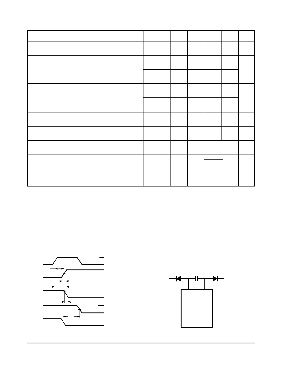
Figure 1. Switching Waveforms
Figure 2. Discharge Protection During Power Down
OSCin
Aout
OSCin
Ain
VDD
0 V
VDD
0 V
VDD
0 V
50%
90%
50%
10%
tr
tf
tPHL
90%
10%
50%
tsu
50%
D1
D2
Cext
9
7
OSCin
OSCout
MC14490
tPLH
VDD
相关PDF资料 |
PDF描述 |
|---|---|
| MAX202ESE+T | IC TXRX RS-232 W/CAP 16-SOIC |
| VE-25T-MX-F1 | CONVERTER MOD DC/DC 6.5V 75W |
| MS27656T13F8PA | CONN RCPT 8POS WALL MNT W/PINS |
| V72C12M150B3 | CONVERTER MOD DC/DC 12V 150W |
| MS27484T8B44S | CONN PLUG 4POS STRAIGHT W/SCKT |
相关代理商/技术参数 |
参数描述 |
|---|---|
| MC14490DWG | 制造商:ON Semiconductor 功能描述:Gate / Inverter Logic IC Package/Case:16 |
| MC14490DWR2 | 功能描述:算数逻辑单元 - ALU LOG CMOS 3-18V HEX BOUNCE ELIMINATOR RoHS:否 制造商:ON Semiconductor 高电平输出电流: 低电平输出电流: 传播延迟时间: 电源电压-最大:18 V 电源电压-最小:3 V 封装 / 箱体:SOIC-16 Wide 最大工作温度:+ 125 C 封装:Reel |
| MC14490DWR2G | 功能描述:算数逻辑单元 - ALU LOG CMOS 3-18V HEX BOUNCE ELIMINATOR RoHS:否 制造商:ON Semiconductor 高电平输出电流: 低电平输出电流: 传播延迟时间: 电源电压-最大:18 V 电源电压-最小:3 V 封装 / 箱体:SOIC-16 Wide 最大工作温度:+ 125 C 封装:Reel |
| MC14490F | 功能描述:算数逻辑单元 - ALU LOG CMOS 3-18V HEX BOUNCE ELIMINATOR RoHS:否 制造商:ON Semiconductor 高电平输出电流: 低电平输出电流: 传播延迟时间: 电源电压-最大:18 V 电源电压-最小:3 V 封装 / 箱体:SOIC-16 Wide 最大工作温度:+ 125 C 封装:Reel |
| MC14490FEL | 功能描述:算数逻辑单元 - ALU LOG CMOS 3-18V HEX BOUNCE ELIMINATOR RoHS:否 制造商:ON Semiconductor 高电平输出电流: 低电平输出电流: 传播延迟时间: 电源电压-最大:18 V 电源电压-最小:3 V 封装 / 箱体:SOIC-16 Wide 最大工作温度:+ 125 C 封装:Reel |
发布紧急采购,3分钟左右您将得到回复。