- 您现在的位置:买卖IC网 > PDF目录371013 > MC145158-2 (Motorola, Inc.) PLL Frequency Synthesizer(PLL频率合成器) PDF资料下载
参数资料
| 型号: | MC145158-2 |
| 厂商: | Motorola, Inc. |
| 英文描述: | PLL Frequency Synthesizer(PLL频率合成器) |
| 中文描述: | 锁相环频率合成器(PLL频率合成器) |
| 文件页数: | 21/26页 |
| 文件大小: | 423K |
| 代理商: | MC145158-2 |
MC145151–2 through MC145158–2
MOTOROLA
21
CRYSTAL OSCILLATOR CONSIDERATIONS
The following options may be considered to provide a ref-
erence frequency to Motorola’s CMOS frequency synthe-
sizers.
Use of a Hybrid Crystal Oscillator
Commercially available temperature–compensated crystal
oscillators (TCXOs) or crystal–controlled data clock oscilla-
tors provide very stable reference frequencies. An oscillator
capable of sinking and sourcing 50
μ
A at CMOS logic levels
may be direct or dc coupled to OSCin. In general, the highest
frequency capability is obtained utilizing a direct–coupled
square wave having a rail–to–rail (VDD to VSS) voltage
swing. If the oscillator does not have CMOS logic levels on
the outputs, capacitive or ac coupling to OSCin may be used.
OSCout, an unbuffered output, should be left floating.
For additional information about TCXOs and data clock
oscillators, please consult the latest version of the eem Elec-
tronic Engineers Master Catalog,the Gold Book,or similar
publications.
Design an Off–Chip Reference
The user may design an off–chip crystal oscillator using
ICs specifically developed for crystal oscillator applications,
such as the MC12061 MECL device. The reference signal
from the MECL device is ac coupled to OSCin. For large am-
plitude signals (standard CMOS logic levels), dc coupling is
used. OSCout, an unbuffered output, should be left floating.
In general, the highest frequency capability is obtained with a
direct–coupled square wave having rail–to–rail voltage
swing.
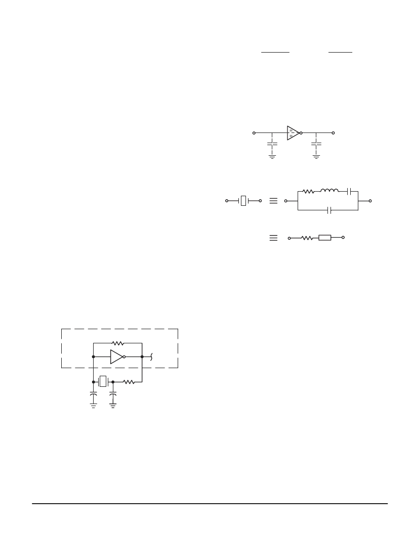
Use of the On–Chip Oscillator Circuitry
The on–chip amplifier (a digital inverter) along with an ap-
propriate crystal may be used to provide a reference source
frequency. A fundamental mode crystal, parallel resonant at
the desired operating frequency, should be connected as
shown in Figure 10.
Figure 10. Pierce Crystal Oscillator Circuit
R1*
C2
C1
FREQUENCY
SYNTHESIZER
OSCout
OSCin
* May be deleted in certain cases. See text.
Rf
For VDD = 5.0 V, the crystal should be specified for a load-
ing capacitance, CL, which does not exceed 32 pF for fre-
quencies to approximately 8.0 MHz, 20 pF for frequencies in
the area of 8.0 to 15 MHz, and 10 pF for higher frequencies.
These are guidelines that provide a reasonable compromise
between IC capacitance, drive capability, swamping varia-
tions in stray and IC input/output capacitance, and realistic
CL values. The shunt load capacitance, CL, presented
across the crystal can be estimated to be:
CinCout
Cin + Cout
where
Cin= 5 pF (see Figure 11)
Cout= 6 pF (see Figure 11)
Ca= 1 pF (see Figure 11)
CO= the crystal’s holder capacitance
(see Figure 12)
C1 and C2 = external capacitors (see Figure 10)
CL =
+ Ca + Co +C1 + C2
C2
Figure 11. Parasitic Capacitances of the Amplifier
Cin
Cout
Ca
Figure 12. Equivalent Crystal Networks
NOTE: Values are supplied by crystal manufacturer
(parallel resonant crystal).
2
1
2
1
2
1
RS
LS
CS
Re
Xe
CO
The oscillator can be “trimmed” on–frequency by making a
portion or all of C1 variable. The crystal and associated com-
ponents must be located as close as possible to the OSCin
and OSCout pins to minimize distortion, stray capacitance,
stray inductance, and startup stabilization time. In some
cases, stray capacitance should be added to the value for Cin
and Cout.
Power is dissipated in the effective series resistance of the
crystal, Re, in Figure 12. The drive level specified by the crys-
tal manufacturer is the maximum stress that a crystal can
withstand without damage or excessive shift in frequency. R1
in Figure 10 limits the drive level. The use of R1 may not be
necessary in some cases (i.e., R1 = 0
).
To verify that the maximum dc supply voltage does not
overdrive the crystal, monitor the output frequency as a func-
tion of voltage at OSCout. (Care should be taken to minimize
loading.) The frequency should increase very slightly as the
dc supply voltage is increased. An overdriven crystal will de-
crease in frequency or become unstable with an increase in
supply voltage. The operating supply voltage must be re-
duced or R1 must be increased in value if the overdriven
condition exists. The user should note that the oscillator
start–up time is proportional to the value of R1.
Through the process of supplying crystals for use with
CMOS inverters, many crystal manufacturers have devel-
oped expertise in CMOS oscillator design with crystals. Dis-
cussions with such manufacturers can prove very helpful
(see Table 1).
相关PDF资料 |
PDF描述 |
|---|---|
| MC145158DW | Serial-Input PLL Frequency Synthesizer |
| MC145158P2 | Parallel-Input PLL Frequency Synthesizer |
| MC145158FN | Non-inverting Dual High-Speed MOSFET Drivers with Internal Regulator 8-PDIP |
| MC145158P | Serial-Input PLL Frequency Synthesizer |
| MC145158DW2 | Parallel-Input PLL Frequency Synthesizer |
相关代理商/技术参数 |
参数描述 |
|---|---|
| MC145158DW2 | 功能描述:IC SER-IN PLL FREQ SYNTH 16-SOIC RoHS:否 类别:集成电路 (IC) >> 时钟/计时 - 时钟发生器,PLL,频率合成器 系列:- 标准包装:39 系列:- 类型:* PLL:带旁路 输入:时钟 输出:时钟 电路数:1 比率 - 输入:输出:1:10 差分 - 输入:输出:是/是 频率 - 最大:170MHz 除法器/乘法器:无/无 电源电压:2.375 V ~ 3.465 V 工作温度:0°C ~ 70°C 安装类型:* 封装/外壳:* 供应商设备封装:* 包装:* |
| MC145158DW2R2 | 制造商: 功能描述: 制造商:undefined 功能描述: |
| MC145159FN1R2 | 制造商:Motorola Inc 功能描述: |
| MC145159P1 | 制造商:Motorola Inc 功能描述: |
| MC14515BCP | 功能描述:编码器、解码器、复用器和解复用器 3-18V 4-Bit RoHS:否 制造商:Micrel 产品:Multiplexers 逻辑系列:CMOS 位数: 线路数量(输入/输出):2 / 12 传播延迟时间:350 ps, 400 ps 电源电压-最大:2.625 V, 3.6 V 电源电压-最小:2.375 V, 3 V 最大工作温度:+ 85 C 安装风格:SMD/SMT 封装 / 箱体:QFN-44 封装:Tray |
发布紧急采购,3分钟左右您将得到回复。