- 您现在的位置:买卖IC网 > PDF目录25621 > MC14526BFL1 (ON SEMICONDUCTOR) 4000/14000/40000 SERIES, SYN POSITIVE EDGE TRIGGERED 4-BIT DOWN BINARY COUNTER, PDSO16 PDF资料下载
参数资料
| 型号: | MC14526BFL1 |
| 厂商: | ON SEMICONDUCTOR |
| 元件分类: | 计数器 |
| 英文描述: | 4000/14000/40000 SERIES, SYN POSITIVE EDGE TRIGGERED 4-BIT DOWN BINARY COUNTER, PDSO16 |
| 封装: | EIAJ, PLASTIC, SOIC-16 |
| 文件页数: | 1/14页 |
| 文件大小: | 242K |
| 代理商: | MC14526BFL1 |
Semiconductor Components Industries, LLC, 2000
March, 2000 – Rev. 3
1
Publication Order Number:
MC14526B/D
MC14526B
Presettable 4-Bit Down
Counters
The MC14526B binary counter is constructed with MOS P–channel
and N–channel enhancement mode devices in a monolithic structure.
This device is presettable, cascadable, synchronous down counter
with a decoded “0” state output for divide–by–N applications. In
single stage applications the “0” output is applied to the Preset Enable
input. The Cascade Feedback input allows cascade divide–by–N
operation with no additional gates required. The Inhibit input allows
disabling of the pulse counting function. Inhibit may also be used as a
negative edge clock.
This complementary MOS counter can be used in frequency
synthesizers, phase–locked loops, and other frequency division
applications requiring low power dissipation and/or high noise
immunity.
Supply Voltage Range = 3.0 Vdc to 18 Vdc
Logic Edge–Clocked Design — Incremented on Positive Transition
of Clock or Negative Transition of Inhibit
Asynchronous Preset Enable
Capable of Driving Two Low–power TTL Loads or One Low–power
Schottky TTL Load Over the Rated Temperature Range
MAXIMUM RATINGS (Voltages Referenced to VSS) (Note 2.)
Symbol
Parameter
Value
Unit
VDD
DC Supply Voltage Range
– 0.5 to +18.0
V
Vin, Vout
Input or Output Voltage Range
(DC or Transient)
– 0.5 to VDD + 0.5
V
Iin, Iout
Input or Output Current
(DC or Transient) per Pin
±10
mA
PD
Power Dissipation,
per Package (Note 3.)
500
mW
TA
Operating Temperature Range
– 55 to +125
°C
Tstg
Storage Temperature Range
– 65 to +150
°C
TL
Lead Temperature
(8–Second Soldering)
260
°C
2. Maximum Ratings are those values beyond which damage to the device
may occur.
3. Temperature Derating:
Plastic “P and D/DW” Packages: – 7.0 mW/
_C From 65_C To 125_C
This device contains protection circuitry to guard against damage due to high
static voltages or electric fields. However, precautions must be taken to avoid
applications of any voltage higher than maximum rated voltages to this
high–impedance circuit. For proper operation, Vin and Vout should be constrained
to the range VSS v (Vin or Vout) v VDD.
Unused inputs must always be tied to an appropriate logic voltage level (e.g.,
either VSS or VDD). Unused outputs must be left open.
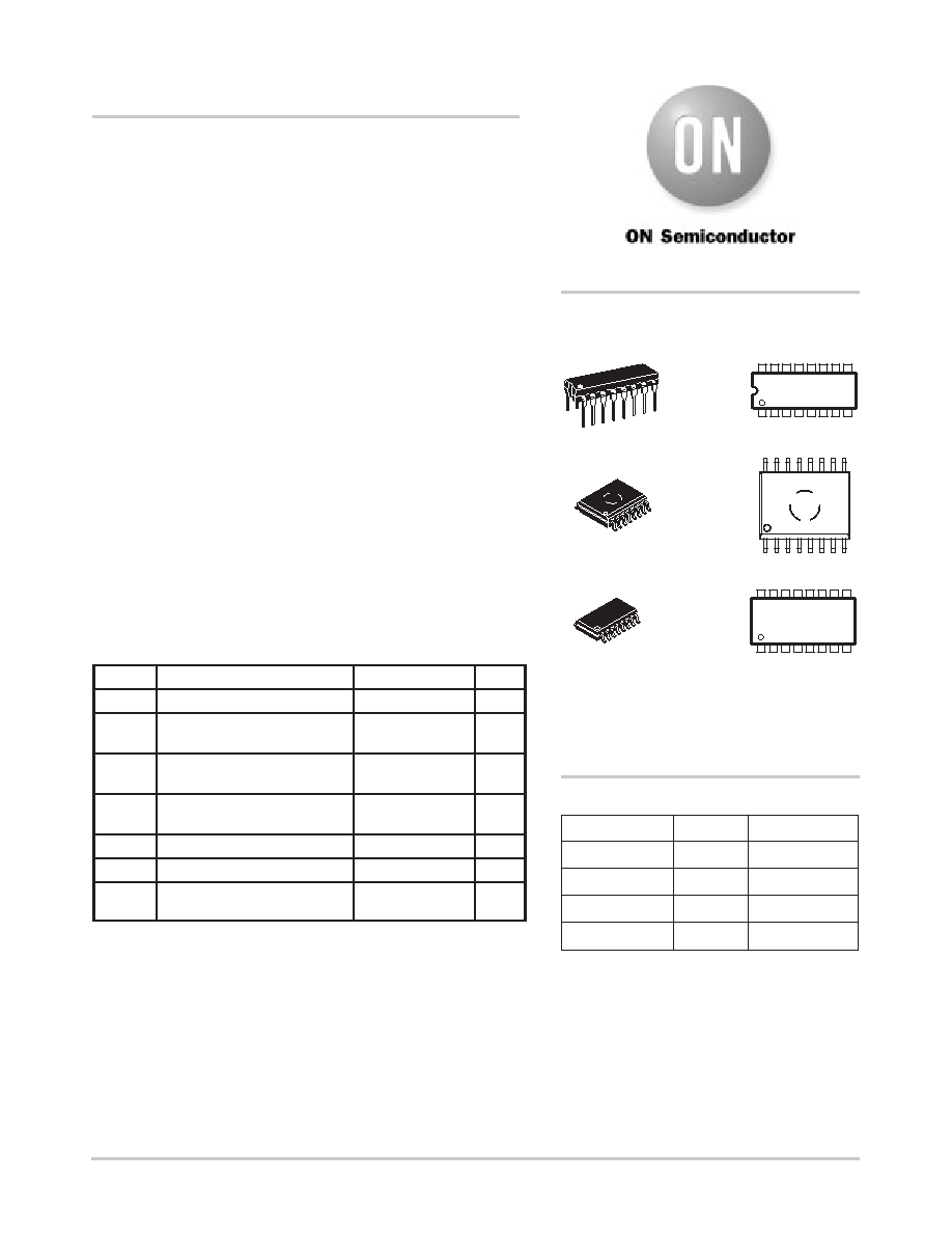
http://onsemi.com
A
= Assembly Location
WL or L
= Wafer Lot
YY or Y
= Year
WW or W = Work Week
Device
Package
Shipping
ORDERING INFORMATION
MC14526BCP
PDIP–16
2000/Box
MC14526BDW
SOIC–16
47/Rail
MARKING
DIAGRAMS
1
16
PDIP–16
P SUFFIX
CASE 648
MC14526BCP
AWLYYWW
MC14526BDWR2
SOIC–16
1000/Tape & Reel
SOIC–16
DW SUFFIX
CASE 751G
1
16
14526B
AWLYYWW
1. For ordering information on the EIAJ version of
the SOIC packages, please contact your local
ON Semiconductor representative.
SOEIAJ–16
F SUFFIX
CASE 966
1
16
MC14526B
AWLYWW
MC14526BF
SOEIAJ–16
See Note 1.
相关PDF资料 |
PDF描述 |
|---|---|
| MC14532BFR2 | 4000/14000/40000 SERIES, 8-BIT ENCODER, PDSO16 |
| MC14543BFL1 | 4000/14000/40000 SERIES, SEVEN SEGMENT DECODER/DRIVER, CONFIGURABLE OUTPUT, PDSO16 |
| MC14557BCPDS | 4000/14000/40000 SERIES, 64-BIT RIGHT SERIAL IN SERIAL OUT SHIFT REGISTER, COMPLEMENTARY OUTPUT, PDIP16 |
| MC14562BCPD | 4000/14000/40000 SERIES, 128-BIT RIGHT SERIAL IN SERIAL OUT SHIFT REGISTER, TRUE OUTPUT, PDIP14 |
| MC14569BDWR2 | 4000/14000/40000 SERIES, ASYN POSITIVE EDGE TRIGGERED 4-BIT UP BINARY COUNTER, PDSO16 |
相关代理商/技术参数 |
参数描述 |
|---|---|
| MC14526BFR1 | 制造商:Rochester Electronics LLC 功能描述:- Bulk |
| MC14527BCP | 制造商:Freescale Semiconductor 功能描述: |
| MC14528 | 制造商:Misc 功能描述: |
| MC14528BCP | 功能描述:单稳态多谐振荡器 3-18V Dual RoHS:否 制造商:Texas Instruments 每芯片元件:1 逻辑系列:LVC 逻辑类型:Monostable Multivibrator 封装 / 箱体:SSOP-8 传播延迟时间:18.6 ns 高电平输出电流:- 32 mA 低电平输出电流:32 mA 电源电压-最大:5.5 V 电源电压-最小:1.65 V 最大功率耗散: 最大工作温度:+ 85 C 最小工作温度:- 40 C 封装:Reel |
| MC14528BCPG | 功能描述:单稳态多谐振荡器 3-18V Dual MonoStable RoHS:否 制造商:Texas Instruments 每芯片元件:1 逻辑系列:LVC 逻辑类型:Monostable Multivibrator 封装 / 箱体:SSOP-8 传播延迟时间:18.6 ns 高电平输出电流:- 32 mA 低电平输出电流:32 mA 电源电压-最大:5.5 V 电源电压-最小:1.65 V 最大功率耗散: 最大工作温度:+ 85 C 最小工作温度:- 40 C 封装:Reel |
发布紧急采购,3分钟左右您将得到回复。