参数资料
| 型号: | MC14538BDR2 |
| 厂商: | ON Semiconductor |
| 文件页数: | 13/14页 |
| 文件大小: | 0K |
| 描述: | IC MULTIVIBRATR DUAL CMOS 16SOIC |
| 标准包装: | 1 |
| 系列: | 4000B |
| 逻辑类型: | 单稳态 |
| 独立电路: | 2 |
| 施密特触发器输入: | 无 |
| 传输延迟: | 95ns |
| 输出电流高,低: | 8.8mA,8.8mA |
| 电源电压: | 3 V ~ 18 V |
| 工作温度: | -55°C ~ 125°C |
| 安装类型: | 表面贴装 |
| 封装/外壳: | 16-SOIC(0.154",3.90mm 宽) |
| 供应商设备封装: | 16-SOIC |
| 包装: | 标准包装 |
| 其它名称: | MC14538BDR2OSDKR |
MC14538B
http://onsemi.com
8
TRIGGER OPERATION
The block diagram of the MC14538B is shown in
Figure 1, with circuit operation following.
As shown in Figure 1 and 10, before an input trigger
occurs, the monostable is in the quiescent state with the Q
output low, and the timing capacitor CX completely charged
to VDD. When the trigger input A goes from VSS to VDD
(while inputs B and Reset are held to VDD) a valid trigger is
recognized, which turns on comparator C1 and Nchannel
transistor N1 . At the same time the output latch is set. With
transistor N1 on, the capacitor CX rapidly discharges toward
VSS until Vref1 is reached. At this point the output of
comparator C1 changes state and transistor N1 turns off.
Comparator C1 then turns off while at the same time
comparator C2 turns on. With transistor N1 off, the capacitor
CX begins to charge through the timing resistor, RX, toward
VDD. When the voltage across CX equals Vref 2, comparator
C2 changes state, causing the output latch to reset (Q goes
low) while at the same time disabling comparator C2 . This
ends at the timing cycle with the monostable in the quiescent
state, waiting for the next trigger.
In the quiescent state, CX is fully charged to VDD causing
the current through resistor RX to be zero. Both comparators
are “off” with total device current due only to reverse
junction leakages. An added feature of the MC14538B is
that the output latch is set via the input trigger without regard
to the capacitor voltage. Thus, propagation delay from
trigger to Q is independent of the value of CX, RX, or the duty
cycle of the input waveform.
RETRIGGER OPERATION
The MC14538B is retriggered if a valid trigger occurs
followed by another valid trigger before the Q output has
returned to the quiescent (zero) state. Any retrigger, after the
timing node voltage at pin 2 or 14 has begun to rise from
Vref 1, but has not yet reached Vref 2, will cause an increase
in output pulse width T. When a valid retrigger is initiated
, the voltage at CX/RX will again drop to Vref 1 before
progressing along the RC charging curve toward VDD. The
Q output will remain high until time T, after the last valid
retrigger.
RESET OPERATION
The MC14538B may be reset during the generation of the
output pulse. In the reset mode of operation, an input pulse
on Reset sets the reset latch and causes the capacitor to be
fast charged to VDD by turning on transistor P1 . When the
voltage on the capacitor reaches Vref 2, the reset latch will
clear, and will then be ready to accept another pulse. It the
Reset input is held low, any trigger inputs that occur will be
inhibited and the Q and Q outputs of the output latch will not
change. Since the Q output is reset when an input low level
is detected on the Reset input, the output pulse T can be made
significantly shorter than the minimum pulse width
specification.
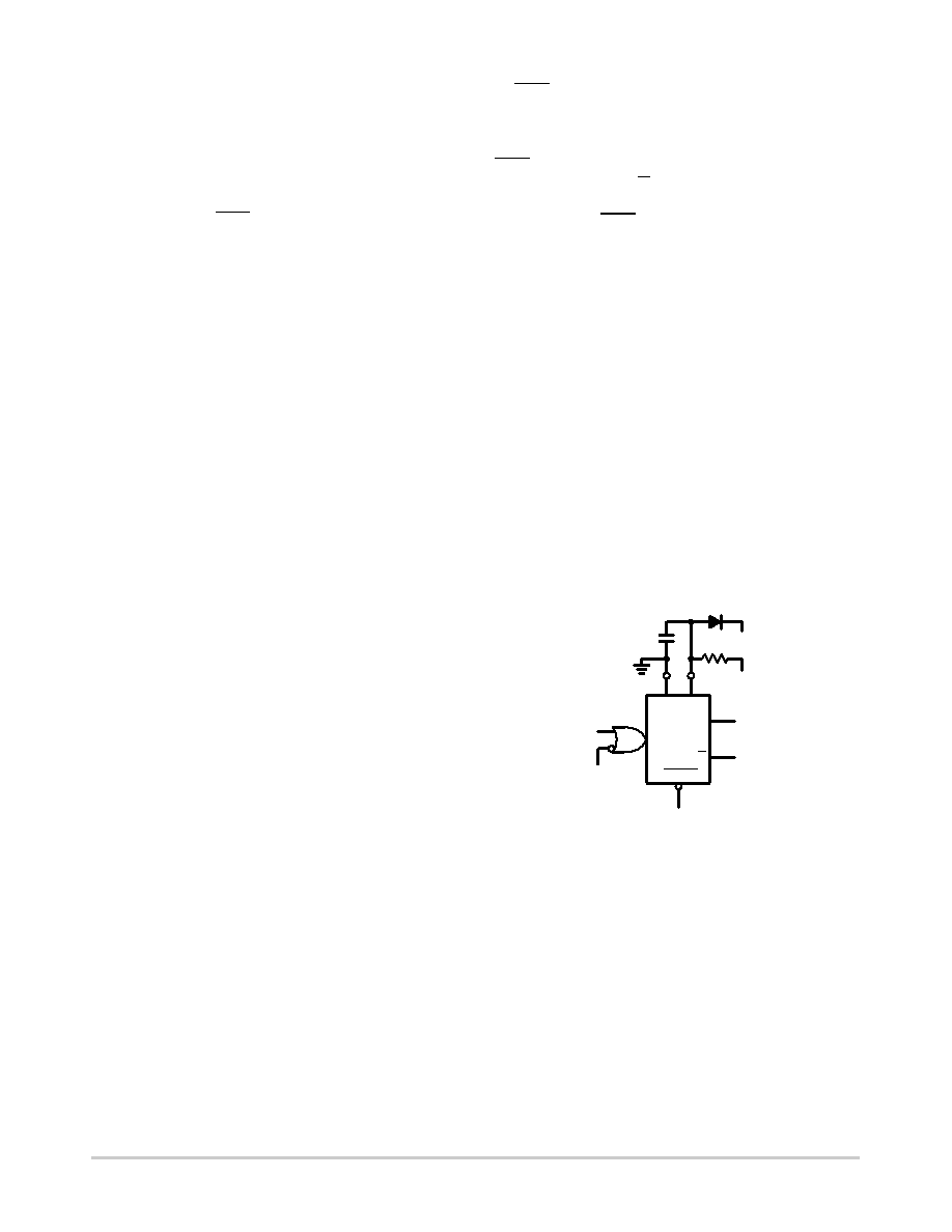
POWERDOWN CONSIDERATIONS
Large capacitance values can cause problems due to the
large amount of energy stored. When a system containing
the MC14538B is powered down, the capacitor voltage may
discharge from VDD through the standard protection diodes
at pin 2 or 14. Current through the protection diodes should
be limited to 10 mA and therefore the discharge time of the
VDD supply must not be faster than (VDD). (C)/(10 mA).
For example, if VDD = 10 V and CX = 10 mF, the VDD supply
should discharge no faster than (10 V) x (10
mF)/(10 mA)
= 10 ms. This is normally not a problem since power
supplies are heavily filtered and cannot discharge at this rate.
When a more rapid decrease of VDD to zero volts occurs,
the MC14538B can sustain damage. To avoid this possibility
use an external clamping diode, DX, connected as shown in
Fig. 11.
Figure 11. Use of a Diode to Limit
Power Down Current Surge
VSS
Dx
VDD
Rx
Cx
Q
RESET
相关PDF资料 |
PDF描述 |
|---|---|
| VE-JWD-MW | CONVERTER MOD DC/DC 85V 100W |
| VE-JWB-MW | CONVERTER MOD DC/DC 95V 100W |
| RT0618-23SNH | CONN HSG PLUG 23POS CABLE SKTS |
| RT0718-23SNH | CONN HSG RCPT 23POS JAM NUT SKTS |
| RT0718-23PNH | CONN HSG RCPT 23POS JAM NUT PINS |
相关代理商/技术参数 |
参数描述 |
|---|---|
| MC14538BDR2G | 功能描述:单稳态多谐振荡器 3-18V Dual Precision MonoStable RoHS:否 制造商:Texas Instruments 每芯片元件:1 逻辑系列:LVC 逻辑类型:Monostable Multivibrator 封装 / 箱体:SSOP-8 传播延迟时间:18.6 ns 高电平输出电流:- 32 mA 低电平输出电流:32 mA 电源电压-最大:5.5 V 电源电压-最小:1.65 V 最大功率耗散: 最大工作温度:+ 85 C 最小工作温度:- 40 C 封装:Reel |
| MC14538BDR2G-CUT TAPE | 制造商:ON 功能描述:MC14538B Series 3 to 18 Vdc Dual Precision Monostable - SOIC-16 |
| MC14538BDT | 制造商:ON Semiconductor 功能描述:Monostable Multivibrator Dual 16-Pin TSSOP Rail |
| MC14538BDTR2 | 功能描述:单稳态多谐振荡器 3-18V Dual Precision RoHS:否 制造商:Texas Instruments 每芯片元件:1 逻辑系列:LVC 逻辑类型:Monostable Multivibrator 封装 / 箱体:SSOP-8 传播延迟时间:18.6 ns 高电平输出电流:- 32 mA 低电平输出电流:32 mA 电源电压-最大:5.5 V 电源电压-最小:1.65 V 最大功率耗散: 最大工作温度:+ 85 C 最小工作温度:- 40 C 封装:Reel |
| MC14538BDTR2G | 功能描述:单稳态多谐振荡器 3-18V Dual Precision MonoStable RoHS:否 制造商:Texas Instruments 每芯片元件:1 逻辑系列:LVC 逻辑类型:Monostable Multivibrator 封装 / 箱体:SSOP-8 传播延迟时间:18.6 ns 高电平输出电流:- 32 mA 低电平输出电流:32 mA 电源电压-最大:5.5 V 电源电压-最小:1.65 V 最大功率耗散: 最大工作温度:+ 85 C 最小工作温度:- 40 C 封装:Reel |
发布紧急采购,3分钟左右您将得到回复。