- 您现在的位置:买卖IC网 > PDF目录11407 > MC14551BDR2G (ON Semiconductor)IC MUX/DEMUX QUAD 2X1 16SOIC PDF资料下载
参数资料
| 型号: | MC14551BDR2G |
| 厂商: | ON Semiconductor |
| 文件页数: | 9/10页 |
| 文件大小: | 0K |
| 描述: | IC MUX/DEMUX QUAD 2X1 16SOIC |
| 标准包装: | 1 |
| 系列: | 4000B |
| 功能: | 多路复用器/多路分解器 |
| 电路: | 4 x 2:1 |
| 导通状态电阻: | 280 欧姆 |
| 电压电源: | 双电源 |
| 电压 - 电源,单路/双路(±): | ±3 V ~ 18 V |
| 电流 - 电源: | 360nA |
| 工作温度: | -55°C ~ 125°C |
| 安装类型: | 表面贴装 |
| 封装/外壳: | 16-SOIC(0.154",3.90mm 宽) |
| 供应商设备封装: | 16-SOIC |
| 包装: | 剪切带 (CT) |
| 其它名称: | MC14551BDR2GOSCT |
MC14551B
http://onsemi.com
8
APPLICATIONS INFORMATION
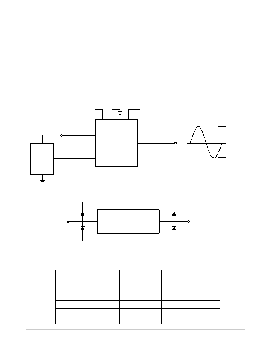
Figure A illustrates use of the onchip level converter
detailed in Figure 2. The 0to5.0 V Digital Control signal is
used to directly control a 9 Vpp analog signal.
The digital control logic levels are determined by VDD and
VSS. The VDD voltage is the logic high voltage; the VSS
voltage is logic low. For the example, VDD = + 5.0 V = logic
high at the control inputs; VSS = GND = 0 V = logic low.
The maximum analog signal level is determined by VDD
and VEE. The VDD voltage determines the maximum
recommended peak above VSS. The VEE voltage determines
the maximum swing below VSS. For the example, VDD – VSS
= 5.0 V maximum swing above VSS; VSS – VEE = 5.0 V
maximum swing below VSS. The example shows a ± 4.5 V
signal which allows a 1/2 V margin at each peak. If voltage
transients above VDD and/or below VEE are anticipated on the
analog channels, external diodes (Dx) are recommended as
shown in Figure B. These diodes should be small signal types
able to absorb the maximum anticipated current surges during
clipping.
The absolute maximum potential difference between VDD
and VEE is 18 V. Most parameters are specified up to 15 V
which is the recommended maximum difference between
VDD and VEE.
Balanced supplies are not required. However, VSS must be
greater than or equal to VEE. For example, VDD = + 10 V, VSS
= + 5.0 V, and VEE = – 3.0 V is acceptable. See the table below.
Figure A. Application Example
EXTERNAL
CMOS
DIGITAL
CIRCUITRY
9 Vp-p
ANALOG SIGNAL
0-TO-5 V DIGITAL
CONTROL SIGNAL
VDD VSS
VEE
SWITCH
I/O
COMMON
O/I
CONTROL
MC14551B
-5 V
+ 5 V
9 Vp-p
ANALOG SIGNAL
+ 4.5 V
- 4.5 V
GND
VDD
VEE
Dx
SWITCH
I/O
COMMON
O/I
Figure B. External Schottky or Germanium Clipping Diodes
+ 5 V
POSSIBLE SUPPLY CONNECTIONS
VDD
In Volts
VSS
In Volts
VEE
In Volts
Control Inputs
Logic High/Logic Low
In Volts
Maximum Analog Signal Range
In Volts
+ 8
0
– 8
+ 8/0
+ 8 to – 8 = 16 Vp–p
+ 5
0
– 12
+ 5/0
+ 5 to – 12 = 17 Vp–p
+ 5
0
0
+ 5/0
+ 5 to 0 = 5 Vp–p
+ 5
0
– 5
+ 5/0
+ 5 to – 5 = 10 Vp–p
+ 10
– 5
+ 10/ + 5
+ 10 to – 5 = 15 Vp–p
相关PDF资料 |
PDF描述 |
|---|---|
| MAX4564EKA+T | IC SWITCH ANLG DUAL SPDT SOT23-8 |
| VE-2NT-IY | CONVERTER MOD DC/DC 6.5V 50W |
| VE-2NT-EU-B1 | CONVERTER MOD DC/DC 6.5V 200W |
| PIC18F65K80-H/PT | IC MCU PIC 32KB FLASH 64TQFP |
| PIC18F86K90-E/PT | IC MCU 8BIT 64KB FLASH 80TQFP |
相关代理商/技术参数 |
参数描述 |
|---|---|
| MC14551BF | 功能描述:多路器开关 IC 3-18V Quad 2 CHNL RoHS:否 制造商:Texas Instruments 通道数量:1 开关数量:4 开启电阻(最大值):7 Ohms 开启时间(最大值): 关闭时间(最大值): 传播延迟时间:0.25 ns 工作电源电压:2.3 V to 3.6 V 工作电源电流: 最大工作温度:+ 85 C 安装风格:SMD/SMT 封装 / 箱体:UQFN-16 |
| MC14551BFEL | 功能描述:多路器开关 IC 3-18V Quad 2 CHNL RoHS:否 制造商:Texas Instruments 通道数量:1 开关数量:4 开启电阻(最大值):7 Ohms 开启时间(最大值): 关闭时间(最大值): 传播延迟时间:0.25 ns 工作电源电压:2.3 V to 3.6 V 工作电源电流: 最大工作温度:+ 85 C 安装风格:SMD/SMT 封装 / 箱体:UQFN-16 |
| MC14551BFELG | 功能描述:多路器开关 IC 3-18V Quad 2 CHNL Mux/Demux -55 to 125 RoHS:否 制造商:Texas Instruments 通道数量:1 开关数量:4 开启电阻(最大值):7 Ohms 开启时间(最大值): 关闭时间(最大值): 传播延迟时间:0.25 ns 工作电源电压:2.3 V to 3.6 V 工作电源电流: 最大工作温度:+ 85 C 安装风格:SMD/SMT 封装 / 箱体:UQFN-16 |
| MC14551BFG | 功能描述:多路器开关 IC 3-18V Quad 2 CHNL Mux/Demux -55 to 125 RoHS:否 制造商:Texas Instruments 通道数量:1 开关数量:4 开启电阻(最大值):7 Ohms 开启时间(最大值): 关闭时间(最大值): 传播延迟时间:0.25 ns 工作电源电压:2.3 V to 3.6 V 工作电源电流: 最大工作温度:+ 85 C 安装风格:SMD/SMT 封装 / 箱体:UQFN-16 |
| MC14551C38E WAF | 制造商:ON Semiconductor 功能描述: |
发布紧急采购,3分钟左右您将得到回复。