参数资料
| 型号: | MC14572UBDR2G |
| 厂商: | ON Semiconductor |
| 文件页数: | 1/6页 |
| 文件大小: | 0K |
| 描述: | IC GATE HEX NAND/NOR/INV 16-SOIC |
| 标准包装: | 2,500 |
| 系列: | 4000B |
| 逻辑类型: | 与非/或非反相门 |
| 电路数: | 6 |
| 输入数: | 8 输入(1,1,2,2,1,1) |
| 施密特触发器输入: | 无 |
| 输出类型: | 单端 |
| 输出电流高,低: | 3.5mA,8.8mA |
| 电源电压: | 3 V ~ 18 V |
| 工作温度: | -55°C ~ 125°C |
| 安装类型: | 表面贴装 |
| 封装/外壳: | 16-SOIC(0.154",3.90mm 宽) |
| 供应商设备封装: | 16-SOIC |
| 包装: | 带卷 (TR) |
Semiconductor Components Industries, LLC, 2013
May, 2013 Rev. 8
1
Publication Order Number:
MC14572UB/D
MC14572UB
Hex Gate
The MC14572UB hex functional gate is constructed with MOS
Pchannel and Nchannel enhancement mode devices in a single
monolithic structure. These complementary MOS logic gates find
primary use where low power dissipation and/or high noise immunity
is desired. The chip contains four inverters, one NOR gate and one
NAND gate.
Features
Diode Protection on All Inputs
Single Supply Operation
Supply Voltage Range = 3.0 Vdc to 18 Vdc
NOR Input Pin Adjacent to VSS Pin to Simplify Use As An Inverter
NAND Input Pin Adjacent to VDD Pin to Simplify Use As An
Inverter
NOR Output Pin Adjacent to Inverter Input Pin For OR Application
NAND Output Pin Adjacent to Inverter Input Pin For AND
Application
Capable of Driving Two LowPower TTL Loads or One
LowPower Schottky TTL Load over the Rated Temperature
Range
These Devices are PbFree and are RoHS Compliant
NLV Prefix for Automotive and Other Applications Requiring
Unique Site and Control Change Requirements; AECQ100
Qualified and PPAP Capable*
MAXIMUM RATINGS (Voltages Referenced to VSS)
Parameter
Symbol
Value
Unit
DC Supply Voltage Range
VDD
0.5 to +18.0
V
Input or Output Voltage Range
(DC or Transient)
Vin, Vout
0.5 to VDD
+ 0.5
V
Input or Output Current (DC or Transient)
per Pin
Iin, Iout
±10
mA
Power Dissipation, per Package (Note 1)
PD
500
mW
Ambient Temperature Range
TA
55 to +125
°C
Storage Temperature Range
Tstg
65 to +150
°C
Lead Temperature (8Second Soldering)
TL
260
°C
Stresses exceeding Maximum Ratings may damage the device. Maximum
Ratings are stress ratings only. Functional operation above the Recommended
Operating Conditions is not implied. Extended exposure to stresses above the
Recommended Operating Conditions may affect device reliability.
1. Temperature Derating: Plastic “P and D/DW”
Packages: – 7.0 mW/_C From 65_C To 125_C
This device contains protection circuitry to guard against damage due to high
static voltages or electric fields. However, precautions must be taken to avoid
applications of any voltage higher than maximum rated voltages to this
highimpedance circuit. For proper operation, Vin and Vout should be constrained
to the range VSS v (Vin or Vout) v VDD.
Unused inputs must always be tied to an appropriate logic voltage level
(e.g., either VSS or VDD). Unused outputs must be left open.
Device
Package
Shipping
ORDERING INFORMATION
http://onsemi.com
For information on tape and reel specifications,
including part orientation and tape sizes, please
refer to our Tape and Reel Packaging Specifications
Brochure, BRD8011/D.
MC14572UBDR2G
SOIC16
(PbFree)
2500/Tape & Reel
MC14572UBDG
SOIC16
(PbFree)
48 Units / Rail
MC14572UBCPG
PDIP16
(PbFree)
25 Units / Rail
A
= Assembly Location
WL
= Wafer Lot
YY
= Year
WW
= Work Week
G
= PbFree Package
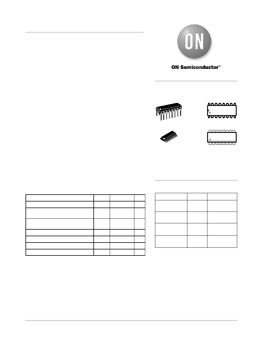
MARKING
DIAGRAMS
PDIP16
P SUFFIX
CASE 648
SOIC16
D SUFFIX
CASE 751B
1
16
14572UBG
AWLYWW
16
1
MC14572UBCP
AWLYYWWG
1
NLV14572UBDR2G* SOIC16
(PbFree)
2500/Tape & Reel
相关PDF资料 |
PDF描述 |
|---|---|
| 2-1879447-0 | RES 39 OHM 200W 5% WW LUG |
| 1-1879447-8 | RES 27 OHM 200W 5% WW LUG |
| 1-1879447-7 | RES 22 OHM 200W 5% WW LUG |
| TXR40AB00-1414BI | ADPTR TINEL LOCK STR SHELL 15, D |
| TXR41AB00-1406AI | ADPTR TINEL LOCK STR SHELL 14,15 |
相关代理商/技术参数 |
参数描述 |
|---|---|
| MC14573P | 制造商:Motorola 功能描述:4573N |
| MC14574D | 制造商:Rochester Electronics LLC 功能描述:- Bulk |
| MC14575CL | 制造商: 功能描述: 制造商:undefined 功能描述: |
| MC14575CP | 制造商: 功能描述: 制造商:Motorola Inc 功能描述: 制造商:undefined 功能描述: |
| MC14576CFEL | 制造商:Rochester Electronics LLC 功能描述:- Bulk |
发布紧急采购,3分钟左右您将得到回复。