参数资料
| 型号: | MC33160P |
| 厂商: | ON Semiconductor |
| 文件页数: | 5/10页 |
| 文件大小: | 0K |
| 描述: | IC REG VOLT MIC 100MA 5V 16DIP |
| 产品变化通告: | LTB Notification 03/Jan/2008 |
| 标准包装: | 25 |
| 类型: | 稳压器/监控器 |
| 监视电压数目: | 1 |
| 输出: | 开路漏极或开路集电极 |
| 复位: | 低有效 |
| 电压 - 阀值: | 4.55V |
| 工作温度: | -40°C ~ 85°C |
| 安装类型: | 通孔 |
| 封装/外壳: | 16-DIP(0.300",7.62mm) |
| 供应商设备封装: | 16-DIP |
| 包装: | 管件 |
| 其它名称: | MC33160POS |
�� �
�
�MC34160,� MC33160�
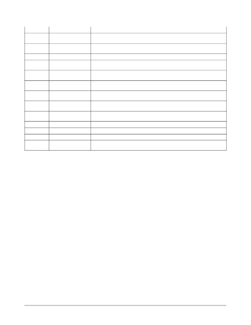
�PIN� FUNCTION� DESCRIPTION�
�Pin�
�1�
�2�
�3�
�4,� 5,� 12,� 13�
�6�
�7�
�8�
�9�
�10�
�11�
�14�
�15�
�16�
�Function�
�Comparator� Inverting�
�Input�
�Comparator� Noninverting�
�Input�
�N.C.�
�GND�
�Comparator� Output�
�Reset�
�Power� Warning�
�Power� Sense�
�Hysteresis� Adjust�
�Regulator� Output�
�V� CC�
�Chip� Disable�
�V� ref�
�Description�
�This� is� the� Uncommitted� Comparator� Inverting� input.� It� is� typically� connected� to� a� resistor�
�divider� to� monitor� a� voltage.�
�This� is� the� Uncommitted� Comparator� Noninverting� input.� It� is� typically� connected� to� a�
�reference� voltage.�
�No� connection.� This� pin� is� not� internally� connected.�
�These� pins� are� the� control� circuit� grounds� and� are� connected� to� the� source� and� load� ground�
�returns.� They� are� part� of� the� IC� lead� frame� and� can� be� used� for� heatsinking.�
�This� is� the� Uncommitted� Comparator� output.� It� is� an� open� collector� sink� ?� only� output� requiring�
�a� pullup� resistor.�
�This� is� the� Reset� Comparator� output.� It� is� an� open� collector� sink� ?� only� output� requiring� a�
�pullup� resistor.�
�This� is� the� Power� Warning� Comparator� output.� It� is� an� open� collector� sink� ?� only� output�
�requiring� a� pullup� resistor.�
�This� is� the� Power� Warning� Comparator� noninverting� input.� It� is� typically� connected� to� a�
�resistor� divider� to� monitor� the� input� power� source� voltage.�
�The� Power� Warning� Comparator� hysteresis� is� programmed� by� a� resistor� connected� from� this�
�pin� to� ground.�
�This� is� the� 5.0� V� Regulator� output.�
�This� pin� is� the� positive� supply� input� of� the� control� IC.�
�This� input� is� used� to� switch� the� IC� into� a� standby� mode� turning� off� all� outputs.�
�This� is� the� 2.6� V� Reference� output.� It� is� intended� to� be� used� in� conjunction� with� the� Power�
�Warning� and� Uncommitted� comparators.�
�OPERATING� DESCRIPTION�
�The� MC34160� series� is� a� monolithic� voltage� regulator� and�
�supervisory� circuit� containing� many� of� the� necessary�
�monitoring� functions� required� in� microprocessor� based�
�systems.� It� is� specifically� designed� for� appliance� and�
�industrial� applications,� offering� the� designer� a� cost� effective�
�solution� with� minimal� external� components.� These� devices�
�are� specified� for� operation� over� an� input� voltage� of� 7.0� V� to�
�40� V,� and� with� a� junction� temperature� of� ?� 40� °� to� +150� °� C.� A�
�typical� microprocessor� application� is� shown� in� Figure� 11.�
�Regulator�
�The� 5.0� V� regulator� is� designed� to� source� in� excess� of�
�100� mA� output� current� and� is� short� circuit� protected.� The�
�output� has� a� guaranteed� tolerance� of� ±� 5.0%� over� line,� load,�
�and� temperature.� Internal� thermal� shutdown� circuitry� is�
�included� to� limit� the� maximum� junction� temperature� to� a�
�safe� level.� When� activated,� typically� at� 170� °� C,� the�
�regulator� output� turns� off.�
�In� specific� situations� a� combination� of� input� and� output�
�bypass� capacitors� may� be� required� for� regulator� stability.� If�
�the� regulator� is� located� an� appreciable� distance� (� ≥� 4� ″� )� from�
�the� supply� filter,� an� input� bypass� capacitor� (C� in� )� of� 0.33� m� F�
�or� greater� is� suggested.� Output� capacitance� values� of� less�
�than� 5.0� nF� may� cause� regulator� instability� at� light� load�
�(� ≤� 1.0� mA)� and� cold� temperature.� An� output� bypass�
�capacitor� of� 0.1� m� F� or� greater� is� recommended� to� ensure�
�stability� under� all� load� conditions.� The� capacitors� selected�
�must� provide� good� high� frequency� characteristics.�
�Good� construction� techniques� should� be� used� to�
�minimize� ground� loops� and� lead� resistance� drops� since� the�
�regulator� does� not� have� external� sense� inputs.�
�Reference�
�The� 2.6� V� bandgap� reference� is� short� circuit� protected�
�and� has� a� guaranteed� output� tolerance� of� ±� 5.0%� over� line,�
�load,� and� temperature.� It� is� intended� to� be� used� in�
�conjunction� with� the� Power� Warning� and� Uncommitted�
�comparator.� The� reference� can� source� in� excess� of� 2.0� mA�
�and� sink� a� maximum� of� 10� m� A.� For� additional� current�
�sinking� capability,� an� external� load� resistor� to� ground� must�
�be� used.�
�Reference� biasing� is� internally� derived� from� either� V� CC�
�or� V� O� ,� allowing� proper� operation� if� either� drops� below�
�nominal.�
�Chip� Disable�
�This� input� is� used� to� switch� the� IC� into� a� standby� mode.�
�When� activated,� internal� biasing� for� the� entire� die� is�
�removed� causing� all� outputs� to� turn� off.� This� reduces� the�
�power� supply� current� (I� CC� )� to� less� than� 0.3� mA.�
�http://onsemi.com�
�5�
�相关PDF资料 |
PDF描述 |
|---|---|
| AP1184K5-50L-13 | IC REG LDO 5V 4A TO263-5L |
| RYM28DTAH | CONN EDGECARD 56POS R/A .156 SLD |
| MC34160P | IC REG/SUPERVSRY 5V 100MA 16DIP |
| AP1184K5-50L-U | IC REG LDO 5V 4A TO263-5 |
| LT3080EQ#PBF | IC REG LDO ADJ 1.1A 5-DDPAK |
相关代理商/技术参数 |
参数描述 |
|---|---|
| MC33160PG | 功能描述:线性稳压器 - 标准 5V 100mA Supervisor RoHS:否 制造商:STMicroelectronics 输出类型: 极性: 输出电压:1.8 V 输出电流:150 mA 负载调节: 最大输入电压:5.5 V 线路调整率: 最大工作温度:+ 125 C 安装风格:SMD/SMT 封装 / 箱体:SOT-323-5L |
| MC33161 | 制造商:SPC Multicomp 功能描述:FUSE RESETTABLE RADIAL 1.85A 制造商:SPC Multicomp 功能描述:FUSE, PTC RESET, RADIAL, 30V, 1.85A 制造商:SPC Multicomp 功能描述:RESETTABLE FUSE RADIAL 1.85A 制造商:SPC Multicomp 功能描述:FUSE, PTC RESET, 30V, 1.85A, RADIAL; Holding Current:1.85A; Tripping Current:3.7A; Initial Resistance Max:0.09ohm; Operating Voltage:30V; Series:FRU; PTC Fuse Case:Radial Leaded; External Depth:3mm; Initial Resistance Min:0.03ohm ;RoHS Compliant: Yes |
| MC33161 | 制造商:SPC Multicomp 功能描述:PTC Resettable Fuse |
| MC33161D | 功能描述:监控电路 Universal Voltage RoHS:否 制造商:STMicroelectronics 监测电压数: 监测电压: 欠电压阈值: 过电压阈值: 输出类型:Active Low, Open Drain 人工复位:Resettable 监视器:No Watchdog 电池备用开关:No Backup 上电复位延迟(典型值):10 s 电源电压-最大:5.5 V 最大工作温度:+ 85 C 安装风格:SMD/SMT 封装 / 箱体:UDFN-6 封装:Reel |
| MC33161DG | 功能描述:监控电路 Universal Voltage Monitor RoHS:否 制造商:STMicroelectronics 监测电压数: 监测电压: 欠电压阈值: 过电压阈值: 输出类型:Active Low, Open Drain 人工复位:Resettable 监视器:No Watchdog 电池备用开关:No Backup 上电复位延迟(典型值):10 s 电源电压-最大:5.5 V 最大工作温度:+ 85 C 安装风格:SMD/SMT 封装 / 箱体:UDFN-6 封装:Reel |
发布紧急采购,3分钟左右您将得到回复。