- 您现在的位置:买卖IC网 > PDF目录379309 > MC33169DTB-4.0 (ON SEMICONDUCTOR) GaAs POWER AMPLIFIER SUPPORT IC PDF资料下载
参数资料
| 型号: | MC33169DTB-4.0 |
| 厂商: | ON SEMICONDUCTOR |
| 英文描述: | GaAs POWER AMPLIFIER SUPPORT IC |
| 中文描述: | 砷化镓功率放大器支持IC |
| 文件页数: | 5/12页 |
| 文件大小: | 206K |
| 代理商: | MC33169DTB-4.0 |
MC33169
5
MOTOROLA ANALOG IC DEVICE DATA
PIN FUNCTION DESCRIPTION
Pin
Name
Description
1
C2 Input
This is the positive pin for the charge pump capacitor in the voltage doubler.
2
C1/C2
This is the negative pin for the charge pump capacitors.
3
C1 Input
This is the positive pin for the charge pump capacitor in the voltage tripler.
4
VO Output
It delivers a regulated negative voltage of –4.0 V or –2.5 V depending on the product version. It can
source an output current in excess of 5.0 mA.
5
VO Charge Pump
Capacitor +
This is the positive pin for the capacitor in the inverting charge pump.
6
Gnd
This pin is Ground for both signal and power circuitry.
7
VO Charge Pump
Capacitor –
This is the negative pin for the capacitor in the inverting charge pump.
8
Gate Drive Output
This is the output of the gate amplifier which directly drives the gate of an N–Channel MOSFET. It can
sink and source peak currents up to 3.0 mA.
9
Tx Power Control
Input
The input signal applied on this pin controls the N–Channel switching MOSFET in follower mode and
therefore, linearly controls the RF output voltage.
10
Sense Input Pin
It senses the negative voltage directly on the Power Amplifier. It is also the input pin of an internal
Undervoltage Lockout circuit which blocks the switching of the N–Channel MOSFET if the sensed
voltage is more positive than –3.0 V (–4.0 V version) or –2.0 V (–2.5 V version).
11
VBB Triple
This is the positive pin of the output filter capacitor in the voltage tripler. The triple voltage at that pin is
used internally to supply the inverting charge pump and the gate amplifier.
12
VBB Double
Idle Mode Input
This is the positive pin of the output filter capacitor in the voltage doubler.
13
This pin is used to set the circuit in Low Power Consumption Standby mode. It is CMOS compatible, i.e.
a voltage lower than 0.5 V applied on this pin makes the device go into Standby mode in which the
current consumption is lower than 1.0
μ
A. The MC33169 is then awakened by a voltage higher than
2.0 V applied on that pin.
14
VCC
This is the supply input pin for the MC33169, VCC voltage ranges from 2.7 V to 7.2 V.
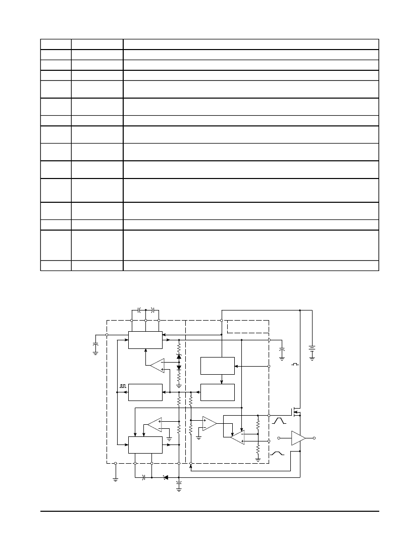
Figure 1. MC33169 Representative Block Diagram
1
2
3
C2
C1
VBB Double
12
Cd
9
Tx(on)
GaAs
PA
RF Out
RF In
10
Vsense
4
5
7
6
Gnd
Cp
Cn
VO
Negative
Charge Pump
Negative Regulator
(–4.0 or –2.5 V)
Gate
Amplifier
Oscillator
Positive
Charge Pump
Positive
Regulator
14
VCC
VBB Triple
11
13
Idle Mode
Input
Ct
+
VBattery
VGout
8
VDD
UVLO
Voltage
Reference
Standby
Circuit
Priority
Management
相关PDF资料 |
PDF描述 |
|---|---|
| MC33169 | GaAs POWER AMPLIFIER SUPPORT IC |
| MC33169DTB-4.0 | GaAs POWER AMPLIFIER SUPPORT IC |
| MC33215B | Telephone Line Interface and Speakerphone Circuit |
| MC33215FB | Telephone Line Interface and Speakerphone Circuit |
| MC33219ADW | VOICE SWITCHED SPEAKERPHONE CIRCUIT |
相关代理商/技术参数 |
参数描述 |
|---|---|
| MC3317 | 制造商:MOTOROLA 制造商全称:Motorola, Inc 功能描述:Amplifiers and Comparators |
| MC33170 | 制造商:SPC Multicomp 功能描述:FUSE RESETTABLE RADIAL 0.17A 制造商:SPC Multicomp 功能描述:FUSE, PTC RESET, RADIAL, 60V, 170MA 制造商:SPC Multicomp 功能描述:RESETTABLE FUSE RADIAL 0.17A 制造商:SPC Multicomp 功能描述:FUSE, PTC RESET, 60V, 170mA, RADIAL; Holding Current:170mA; Tripping Current:340mA; Initial Resistance Max:8ohm; Operating Voltage:60V; Series:FRX; PTC Fuse Case:Radial Leaded; External Depth:3.1mm; Initial Resistance Min:2ohm ;RoHS Compliant: Yes |
| MC33170 | 制造商:SPC Multicomp 功能描述:PTC Resettable Fuse |
| MC33170DTB | 制造商:Rochester Electronics LLC 功能描述:- Bulk |
| MC33170DTBR2 | 制造商:Rochester Electronics LLC 功能描述:- Bulk |
发布紧急采购,3分钟左右您将得到回复。