- 您现在的位置:买卖IC网 > PDF目录359132 > MC33198 (飞思卡尔半导体(中国)有限公司) High Side TMOS Driver(高端TMOS驱动器) PDF资料下载
参数资料
| 型号: | MC33198 |
| 厂商: | 飞思卡尔半导体(中国)有限公司 |
| 英文描述: | High Side TMOS Driver(高端TMOS驱动器) |
| 中文描述: | 高边坡的TMOS驱动器(高端的TMOS驱动器) |
| 文件页数: | 8/11页 |
| 文件大小: | 296K |
| 代理商: | MC33198 |
MC33198
8
MC33198
Pin 1 is connected to the MOSFET source pin. Two
different cases should be considered, MOSFET on or off :
When MOSFET is on and working in normal conditions,
the Vds should be less than the voltage developed at pin 2.
So, the C2 comparator output is low and the status is high. No
current will flow through the pin 8 capacitor.
If the MOSFET encounters an over-load or if the load is shor-
ted to Gnd, the voltage at the source will cross pin 2 voltage
and go below this pin 2 voltage, thereby turning on the C2
comparator. The comparator will pull the status pin 6 low and
will enable the charge of the pin 8 capacitor. When the vol-
tage at the capacitor reaches 5.5V, the C3 comparator will
switch off the MOSFET by disabling the charge pump and
the 110
μ
A current source. The MOSFET gate will be dis-
charged only by the 10
μ
A current source. The MOSFET is
latched off and can be turned back on again by switching
input pin 7 to 0 and back to 1.
When MOSFET is off, we have the same scheme.
In normal condition the load should pull the source voltage
to Gnd, thus C2 comparator output is high and status pin
pulled low. If the load is shorted to V
bat
for instance, source pin
will be higher that pin 2, C2 output comparator is low and
status pin is high. This is summarized in the following table :
Table1
Status Functionality
Operation With Inductive Loads
The device can drive MOSFET in inductive loads
switching applications. In this case, a 1k
resistor should be
connected between source of the MOSFET and device pin 1.
The resistor will limit the current flowing into pin 1 and prevent
MC33198D from damage during switching off of the inductive
load. The gate voltage is internally clamped at - Vbe (0.6V
typical), then the Vds is limited to Vbat + Vbe + Vgson to
prevent excessive power dissipation in the MOSFET. The
load voltage is limited to Vbe + Vgson and allows reasonable
discharge current.
Switching On
The switching on of the MOSFET is ensured by the
internal charge pump. The charge pump response time
versus the MOSFET gate capacitance is shown in table
Dynamic Electrical Characteristics table .
Switching Off
Here two cases have to be discussed ; the normal
switching off of the MOSFET and the switching off under fault
condition. The normal switching off is done by internal pull
down current sources. The value is 110
μ
A and is in fact
composed of two current sources in parallel ; a 100
μ
A and a
10
μ
A source. The 10
μ
A current is always connected to the
gate pin 4 as shown in device block diagram.
Input
Condition
Source
Load
Voltage
C1
Output
Comp
Fault
Pin6
Timer
Pin8
Low
Normal
< Vpin2
High
Low
Low
Low
Short circuit
to V
bat
> Vpin 2
Low
High
Charge
by 10
μ
A
source
High
Normal
> Vpin 2
Low
High
Low
High
Short to
Gnd
or Over load
< Vpin2
High
Low
Charge
by 10
μ
A
source
The 100
μ
A source can be disabled. This is the case when
the MOSFET is switched off under fault conditions. The
device will disable the 100
μ
A current source and the
MOSFET gate will be discharged only by a 10
μ
A current. The
time required to switch off the MOSFET will be much longer in
this case and will result in a lower over-voltage at the
MOSFET, especially when the device drives high inductive
loads.
Off State Operation without V
cc
Connection
When pin 7 is in low state the MOSFET is off. If V
bat
is
present, the gate voltage is discharged by the 110
μ
A current
source. In the case of Vbat disconnection, a self sustaining
5
μ
A pull down current source is incorporated in the device to
ensure that the MOSFET gate capacitor is discharged and
tied below 0.9V. In case of Vcc disconnection, input pin 7 has
no effect on gate voltage which is maintained below 0.9V and
in this case, status pin is high. Low leakage current at pin 2
(10
μ
A max) allows operation with MOSFET and MC33198D
pin 2 permanently connected to battery. Vcc and other
functions can be switched off from the main battery line. See
figure 15
.
PWM Operation
Since the MC33198D charge pump can deliver a high
current, the MOSFET gate can be charged fast enough to
allow PWM operations. The maximum PWM frequency is
dependent on the MOSFET itself and mainly its gate to source
capacitor value. Depending on the PWM frequency, the
switching off time can be long, compared to the on-switching
time response. This is due to the 110
μ
A gate discharge
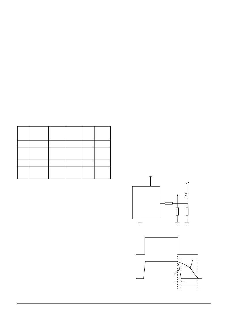
current. To improve this parameter, a resistor can be added in
parallel with the gate of the MOSFET. See figures 13 and 14
below.
Figure13.
Figure14.
1
4
3
Vbat
Vbat
1K
Rg
LOAD
0V
5V
INPUT SIGNAL PIN7
Vcc + 15V typ
0V
Vgate WITHOUT Rgate
Vgate WITH Rgate
Toff
Toff
F
For More Information On This Product,
Go to: www.freescale.com
n
.
相关PDF资料 |
PDF描述 |
|---|---|
| MC33199 | ISO 9141 Serial Link Driver(ISO-9141串行链路驱动器) |
| MC33285 | Dual High Side TMOS Driver(双高端TMOS驱动器) |
| MC33286 | Dual High Side Driver(双高端驱动器) |
| MC33287 | Contact Monitoring and Dual Low Side Protected Driver(接触监测及双低端保护驱动器) |
| MC33288 | Solid State Relay for Automotive Flasher Applications(固态继电器,适用于自动闪光器) |
相关代理商/技术参数 |
参数描述 |
|---|---|
| MC33198 | 制造商:SPC Multicomp 功能描述:PTC Resettable Fuse |
| MC33198D | 制造商:FREESCALE 制造商全称:Freescale Semiconductor, Inc 功能描述:Automotive High-Side TMOS Driver |
| MC33199 | 制造商:SPC Multicomp 功能描述:RESETTABLE FUSE 60V 1.1A |
| MC33199D | 功能描述:DRV AUTO ISO 9141 SER LNK 14SOIC RoHS:否 类别:集成电路 (IC) >> 接口 - 驱动器,接收器,收发器 系列:- 标准包装:1,000 系列:- 类型:收发器 驱动器/接收器数:2/2 规程:RS232 电源电压:3 V ~ 5.5 V 安装类型:表面贴装 封装/外壳:16-SOIC(0.295",7.50mm 宽) 供应商设备封装:16-SOIC 包装:带卷 (TR) |
| MC33199DR2 | 功能描述:IC DRVR SER INK ISO9141 14-SOIC RoHS:否 类别:集成电路 (IC) >> 接口 - 驱动器,接收器,收发器 系列:- 标准包装:1,000 系列:- 类型:收发器 驱动器/接收器数:2/2 规程:RS232 电源电压:3 V ~ 5.5 V 安装类型:表面贴装 封装/外壳:16-SOIC(0.295",7.50mm 宽) 供应商设备封装:16-SOIC 包装:带卷 (TR) |
发布紧急采购,3分钟左右您将得到回复。