- 您现在的位置:买卖IC网 > PDF目录17308 > MC33298P (Freescale Semiconductor)IC SWITCH SERIAL OCTAL 20-DIP PDF资料下载
参数资料
| 型号: | MC33298P |
| 厂商: | Freescale Semiconductor |
| 文件页数: | 22/28页 |
| 文件大小: | 0K |
| 描述: | IC SWITCH SERIAL OCTAL 20-DIP |
| 标准包装: | 18 |
| 类型: | 低端 |
| 输入类型: | SPI |
| 输出数: | 8 |
| 导通状态电阻: | 350 毫欧 |
| 电流 - 输出 / 通道: | 1A |
| 电流 - 峰值输出: | 6A |
| 电源电压: | 9 V ~ 26.5 V |
| 工作温度: | -40°C ~ 125°C |
| 安装类型: | 通孔 |
| 封装/外壳: | 20-DIP(0.300",7.62mm) |
| 供应商设备封装: | 20-DIP |
| 包装: | 管件 |
第1页第2页第3页第4页第5页第6页第7页第8页第9页第10页第11页第12页第13页第14页第15页第16页第17页第18页第19页第20页第21页当前第22页第23页第24页第25页第26页第27页第28页
Analog Integrated Circuit Device Data
Freescale Semiconductor
3
33298
PIN CONNECTIONS
ARCHIVE
INFORMATION
ARCHIVE
INFORMATION
PIN CONNECTIONS
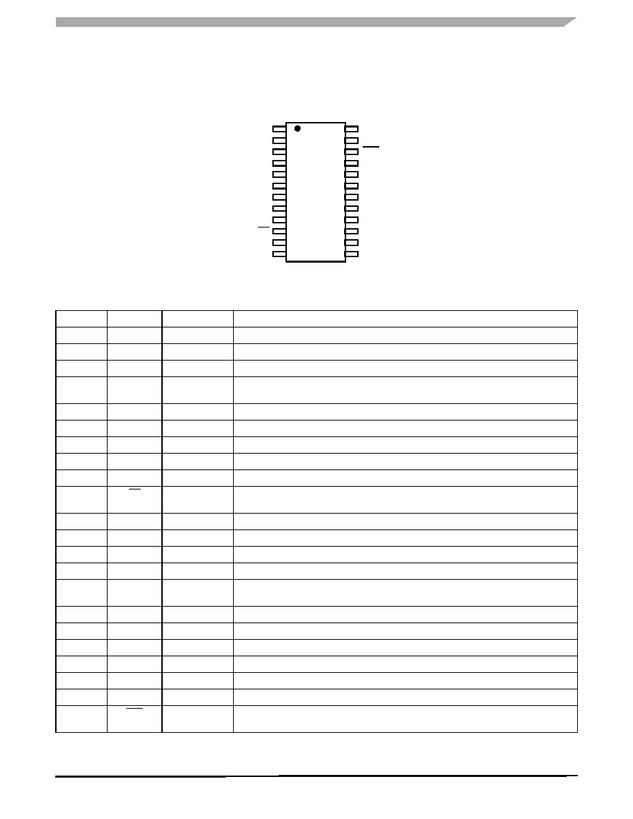
Figure 3. 33298 Pin Connections
Table 2. 33298 Pin Function Description
Pin Number
Pin Name
Formal Name
Definition
1
OP7
Output 7
This pin provides connection to drain of output MOSFET number seven.
2
OP6
Output 6
This pin provides connection to drain of output MOSFET number six.
3
SCLK
System Clock
This pin clocks the internal Shift registers of the 33298.
4
SI
Serial Input
This pin is for the input of serial instruction data. SI information is read on the falling edge of
SCLK.
5
GND
Ground
This pin provides connection to IC Power Ground and functions as part of heat sinking path.
6
GND
Ground
This pin provides connection to IC Power Ground and functions as part of heat sinking path.
7
GND
Ground
This pin provides connection to IC Power Ground and functions as part of heat sinking path.
8
GND
Ground
This pin provides connection to IC Power Ground and functions as part of heat sinking path.
9
SO
Serial Output
This pin is the tri-stateable output from the Shift register.
10
CS
Chip Select
Whenever this pin is in a logic low state, data can be transferred from the MCU to the 33298
through the SI pin and from the 33298 to the MCU through the SO pin.
11
OP5
Output 5
This pin provides connection to drain of output MOSFET number five.
12
OP4
Output 4
This pin provides connection to drain of output MOSFET number four.
13
OP3
Output 3
This pin provides connection to drain of output MOSFET number three.
14
OP2
Output 2
This pin provides connection to drain of output MOSFET number two.
15
SFPD
Short Fault
Protect Disable
This pin is used to prevent the outputs from latching-OFF because of an over current
condition.
16
VDD
Logic Supply
Logic Supply.
17
GND
Ground
This pin provides connection to IC Power Ground and functions as part of heat sinking path.
18
GND
Ground
This pin provides connection to IC Power Ground and functions as part of heat sinking path.
19
GND
Ground
This pin provides connection to IC Power Ground and functions as part of heat sinking path.
20
GND
Ground
This pin provides connection to IC Power Ground and functions as part of heat sinking path.
21
VPWR
Power
Output MOSFET gate drive supply.
22
RST
RESET
This pin is active low. It is used to clear the SPI Shift register, thereby setting all output
switches OFF
.
1
2
3
4
5
6
7
8
9
10
11
12
24
23
22
21
20
19
18
17
16
15
14
13
OP7
OP8
SCLK
SI
GND
SO
CS
OP5
OP4
OP0
OP1
RST
VPWR
GND
VDD
SFPD
OP2
OP3
相关PDF资料 |
PDF描述 |
|---|---|
| MC33298DW | IC SWITCH SERIAL OCTAL 24-SOIC |
| ASPI-0602S-330M-T | INDUCTOR POWER 33UH 0602 SMD |
| ISL6421EVAL1 | EVALUATION BOARD 1 ISL6421 |
| RBC19DREI | CONN EDGECARD 38POS .100 EYELET |
| MC33298DWR2 | IC OCTAL SERIAL SWITCH 24-SOIC |
相关代理商/技术参数 |
参数描述 |
|---|---|
| MC33304P | 制造商:ON Semiconductor 功能描述: |
| MC3330P | 制造商:Rochester Electronics LLC 功能描述:- Bulk |
| MC33340D | 功能描述:电池管理 18V Max NiCD/NiMH RoHS:否 制造商:Texas Instruments 电池类型:Li-Ion 输出电压:5 V 输出电流:4.5 A 工作电源电压:3.9 V to 17 V 最大工作温度:+ 85 C 最小工作温度:- 40 C 封装 / 箱体:VQFN-24 封装:Reel |
| MC33340DG | 功能描述:电池管理 18V Max NiCD/NiMH Fast Charge RoHS:否 制造商:Texas Instruments 电池类型:Li-Ion 输出电压:5 V 输出电流:4.5 A 工作电源电压:3.9 V to 17 V 最大工作温度:+ 85 C 最小工作温度:- 40 C 封装 / 箱体:VQFN-24 封装:Reel |
| MC33340DR2 | 功能描述:电池管理 18V Max NiCD/NiMH RoHS:否 制造商:Texas Instruments 电池类型:Li-Ion 输出电压:5 V 输出电流:4.5 A 工作电源电压:3.9 V to 17 V 最大工作温度:+ 85 C 最小工作温度:- 40 C 封装 / 箱体:VQFN-24 封装:Reel |
发布紧急采购,3分钟左右您将得到回复。