- 您现在的位置:买卖IC网 > PDF目录19623 > MC33362DWR2 (ON Semiconductor)IC SWIT PWM OVP UVLO HV 16SOIC PDF资料下载
参数资料
| 型号: | MC33362DWR2 |
| 厂商: | ON Semiconductor |
| 文件页数: | 7/14页 |
| 文件大小: | 0K |
| 描述: | IC SWIT PWM OVP UVLO HV 16SOIC |
| 产品变化通告: | LTB Notification 03/Jan/2008 |
| 标准包装: | 1 |
| 输出隔离: | 隔离 |
| 频率范围: | 59kHz ~ 315kHz |
| 输入电压: | 9.5 V ~ 40 V |
| 输出电压: | 500V |
| 工作温度: | -25°C ~ 150°C |
| 封装/外壳: | 16-SOIC(0.295",7.50mm 宽)13 引线 |
| 供应商设备封装: | 16-SOIC W |
| 包装: | 标准包装 |
| 其它名称: | MC33362DWR2OSDKR |
��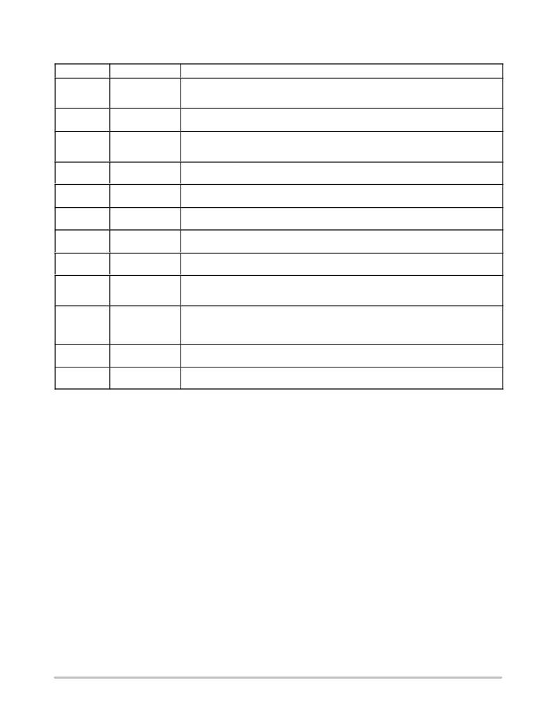 �
�
�MC33362�
�PIN� FUNCTION� DESCRIPTION�
�Pin�
�1�
�2�
�3�
�4,� 5,� 12,� 13�
�6�
�7�
�8�
�9�
�10�
�11�
�14,� 15�
�16�
�Function�
�Startup� Input�
�?�
�V� CC�
�Ground�
�R� T�
�C� T�
�Regulator� Output�
�Compensation�
�Voltage� Feedback�
�Input�
�Overvoltage�
�Protection� Input�
�?�
�Power� Switch� Drain�
�Description�
�This� pin� connects� directly� to� the� rectified� ac� line� voltage� source.� Internally� Pin� 1� is� tied� to� the� drain�
�of� a� high� voltage� startup� MOSFET.� During� startup,� the� MOSFET� supplies� internal� bias,� and�
�charges� an� external� capacitor� that� connects� from� the� V� CC� pin� to� ground.�
�This� pin� has� been� omitted� for� increased� spacing� between� the� rectified� AC� line� voltage� on� Pin� 1�
�and� the� V� CC� potential� on� Pin� 3.�
�This� is� the� positive� supply� voltage� input.� During� startup,� power� is� supplied� to� this� input� from� Pin� 1.�
�When� V� CC� reaches� the� UVLO� upper� threshold,� the� startup� MOSFET� turns� off� and� power� is� sup-�
�plied� from� an� auxiliary� transformer� winding.�
�These� pins� are� the� control� circuit� grounds.� They� are� part� of� the� IC� lead� frame� and� provide� a� ther-�
�mal� path� from� the� die� to� the� printed� circuit� board.�
�Resistor� R� T� connects� from� this� pin� to� ground.� The� value� selected� will� program� the� Current� Limit�
�Comparator� threshold� and� affect� the� Oscillator� frequency.�
�Capacitor� C� T� connects� from� this� pin� to� ground.� The� value� selected,� in� conjunction� with� resistor� R� T� ,�
�programs� the� Oscillator� frequency.�
�This� 6.5� V� output� is� available� for� biasing� external� circuitry.� It� requires� an� external� bypass� capacitor�
�of� at� least� 1.0� m� F� for� stability.�
�This� pin� is� the� Error� Amplifier� output� and� is� made� available� for� loop� compensation.� It� can� be� used�
�as� an� input� to� directly� control� the� PWM� Comparator.�
�This� is� the� inverting� input� of� the� Error� Amplifier.� It� has� a� 2.6� V� threshold� and� normally� connects�
�through� a� resistor� divider� to� the� converter� output,� or� to� a� voltage� that� represents� the� converter�
�output.�
�This� input� provides� runaway� output� voltage� protection� due� to� an� external� component� or� connec-�
�tion� failure� in� the� control� loop� feedback� signal� path.� It� has� a� 2.6� V� threshold� and� normally� con-�
�nects� through� a� resistor� divider� to� the� converter� output,� or� to� a� voltage� that� represents� the� con-�
�verter� output.�
�These� pins� have� been� omitted� for� increased� spacing� between� the� high� voltages� present� on� the�
�Power� Switch� Drain,� and� the� ground� potential� on� Pins� 12� and� 13.�
�This� pin� is� designed� to� directly� drive� the� converter� transformer� and� is� capable� of� switching� a� maxi-�
�mum� of� 500� V� and� 2.0� A.�
�http://onsemi.com�
�7�
�相关PDF资料 |
PDF描述 |
|---|---|
| NDY1205C | CONV DC/DC 3W 12VIN 5VOUT DIP24 |
| VI-202-CY-F1 | CONVERTER MOD DC/DC 15V 50W |
| TAJS685M016RNJ | CAP TANT 6.8UF 16V 20% 1206 |
| M5LV-256/104-7VI | IC CPLD 256MC 104I/O 144TQFP |
| HBC43DRAS-S734 | CONN EDGECARD 86POS .100 R/A PCB |
相关代理商/技术参数 |
参数描述 |
|---|---|
| MC33362DWR2G | 功能描述:直流/直流开关调节器 ANA HI VOLT OFFLN SW REG RoHS:否 制造商:International Rectifier 最大输入电压:21 V 开关频率:1.5 MHz 输出电压:0.5 V to 0.86 V 输出电流:4 A 输出端数量: 最大工作温度: 安装风格:SMD/SMT 封装 / 箱体:PQFN 4 x 5 |
| MC33362XDWR2G | 功能描述:直流/直流开关调节器 ANA HI VOLT OFFLN SW REG RoHS:否 制造商:International Rectifier 最大输入电压:21 V 开关频率:1.5 MHz 输出电压:0.5 V to 0.86 V 输出电流:4 A 输出端数量: 最大工作温度: 安装风格:SMD/SMT 封装 / 箱体:PQFN 4 x 5 |
| MC33363ADW | 功能描述:交流/直流开关转换器 700V 1.5A Switching RoHS:否 制造商:STMicroelectronics 输出电压:800 V 输入/电源电压(最大值):23.5 V 输入/电源电压(最小值):11.5 V 开关频率:115 kHz 电源电流:1.6 mA 工作温度范围:- 40 C to + 150 C 安装风格:SMD/SMT 封装 / 箱体:SSO-10 封装:Reel |
| MC33363ADWG | 功能描述:交流/直流开关转换器 700V 1.5A Switching RoHS:否 制造商:STMicroelectronics 输出电压:800 V 输入/电源电压(最大值):23.5 V 输入/电源电压(最小值):11.5 V 开关频率:115 kHz 电源电流:1.6 mA 工作温度范围:- 40 C to + 150 C 安装风格:SMD/SMT 封装 / 箱体:SSO-10 封装:Reel |
| MC33363ADWR2 | 功能描述:交流/直流开关转换器 700V 1.5A Switching RoHS:否 制造商:STMicroelectronics 输出电压:800 V 输入/电源电压(最大值):23.5 V 输入/电源电压(最小值):11.5 V 开关频率:115 kHz 电源电流:1.6 mA 工作温度范围:- 40 C to + 150 C 安装风格:SMD/SMT 封装 / 箱体:SSO-10 封装:Reel |
发布紧急采购,3分钟左右您将得到回复。