参数资料
| 型号: | MC33363ADW |
| 厂商: | ON Semiconductor |
| 文件页数: | 9/13页 |
| 文件大小: | 0K |
| 描述: | IC SWIT PROG OVP UVLO HV 16SOIC |
| 产品变化通告: | LTB Notification 03/Jan/2008 |
| 标准包装: | 47 |
| 输出隔离: | 隔离 |
| 频率范围: | 59kHz ~ 315kHz |
| 输入电压: | 11.5 V ~ 40 V |
| 输出电压: | 700V |
| 工作温度: | -25°C ~ 125°C |
| 封装/外壳: | 16-SOIC(0.295",7.50mm 宽)13 引线 |
| 供应商设备封装: | 16-SOIC W |
| 包装: | 管件 |
�� �
�
�MC33363A�
�OPERATING� DESCRIPTION�
�Introduction�
�The� MC33363A� represents� a� new� higher� level� of�
�integration� by� providing� all� the� active� high� voltage� power,�
�control,� and� protection� circuitry� required� for�
�implementation� of� a� flyback� or� forward� converter� on� a� single�
�monolithic� chip.� This� device� is� designed� for� direct� operation�
�The� formula� for� the� charge/discharge� current� along� with�
�the� oscillator� frequency� are� given� below.� The� frequency�
�formula� is� a� first� order� approximation� and� is� accurate� for� C� T�
�values� greater� than� 500� pF.� For� smaller� values� of� C� T� ,� refer�
�to� Figure� 2.� Note� that� resistor� R� T� also� programs� the� Current�
�Limit� Comparator� threshold.�
�=� R�
�T�
�from� a� rectified� 240� Vac� line� source� and� requires� a� minimum�
�number� of� external� components� to� implement� a� complete�
�converter.� A� description� of� each� of� the� functional� blocks� is�
�I�
�chg� ∕� dscg�
�5.4�
�T�
�f� ≈�
�I�
�chg� ∕� dscg�
�4C�
�Regulator� Output�
�2.25� I�
�RC� 6� Current�
�R� T�
�Blanking�
�C� T�
�Pulse�
�?� ?�
�RT� --� 1.14�
�1000�
�pk�
�given� below,� and� the� representative� block� and� timing�
�diagrams� are� shown� in� Figures� 19� and� 20.�
�Oscillator� and� Current� Mirror�
�The� oscillator� frequency� is� controlled� by� the� values�
�selected� for� the� timing� components� R� T� and� C� T� .� Resistor� R� T�
�programs� the� oscillator� charge/discharge� current� via� the�
�Current� Mirror� 4� I� output,� Figure� 4.� Capacitor� C� T� is� charged�
�and� discharged� by� an� equal� magnitude� internal� current�
�source� and� sink.� This� generates� a� symmetrical� 50%�
�duty� cycle� waveform� at� Pin� 7,� with� a� peak� and� valley�
�threshold� of� 2.6� V� and� 0.6� V� respectively.� During� the�
�discharge� of� C� T� ,� the� oscillator� generates� an� internal� blanking�
�pulse� that� holds� the� inverting� input� of� the� AND� gate�
�driver� high.� This� causes� the� Power� Switch� gate� drive� to� be�
�held� in� a� low� state,� thus� producing� a� well� controlled� amount�
�of� output� deadtime.� The� amount� of� deadtime� is� relatively�
�constant� with� respect� to� the� oscillator� frequency� when�
�operating� below� 1.0� MHz.� The� maximum� Power� Switch�
�duty� cycle� at� Pin� 16� can� be� modified� from� the� internal� 50%�
�limit� by� providing� an� additional� charge� or� discharge� current�
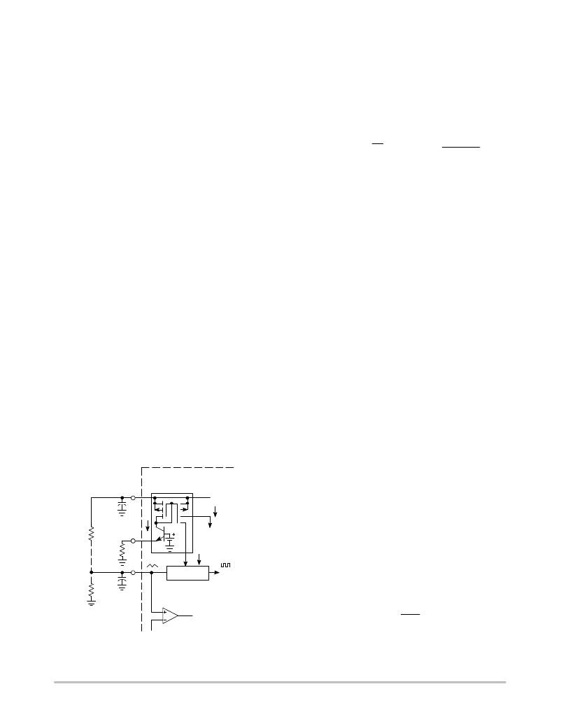
�path� to� C� T� ,� Figure� 21.� In� order� to� increase� the� maximum� duty�
�cycle,� a� discharge� current� resistor� R� D� is� connected� from�
�Pin� 7� to� ground.� To� decrease� the� maximum� duty� cycle,� a�
�charge� current� resistor� R� C� is� connected� from� Pin� 7� to� the�
�Regulator� Output.� Figure� 5� shows� an� obtainable� range� of�
�maximum� output� duty� cycle� versus� the� ratio� of� either� R� C� or�
�R� D� with� respect� to� R� T� .�
�Current�
�Mirror�
�1.0� 8�
�I�
�Limit�
�Reference�
�4I�
�Oscillator�
�7�
�RD�
�PWM�
�Comparator�
�Figure� 21.� Maximum� Duty� Cycle� Modification�
�PWM� Comparator� and� Latch�
�The� pulse� width� modulator� consists� of� a� comparator� with�
�the� oscillator� ramp� voltage� applied� to� the� non--inverting�
�input,� while� the� error� amplifier� output� is� applied� into� the�
�inverting� input.� The� Oscillator� applies� a� set� pulse� to� the�
�PWM� Latch� while� C� T� is� discharging,� and� upon� reaching� the�
�valley� voltage,� Power� Switch� conduction� is� initiated.� When�
�C� T� charges� to� a� voltage� that� exceeds� the� error� amplifier�
�output,� the� PWM� Latch� is� reset,� thus� terminating� Power�
�Switch� conduction� for� the� duration� of� the� oscillator� ramp--up�
�period.� This� PWM� Comparator/Latch� combination�
�prevents� multiple� output� pulses� during� a� given� oscillator�
�clock� cycle.� The� timing� diagram� shown� in� Figure� 20�
�illustrates� the� Power� Switch� duty� cycle� behavior� versus� the�
�Compensation� voltage.�
�Current� Limit� Comparator� and� Power� Switch�
�The� MC33363A� uses� cycle--by--cycle� current� limiting� as�
�a� means� of� protecting� the� output� switch� transistor� from�
�overstress.� Each� on--cycle� is� treated� as� a� separate� situation.�
�Current� limiting� is� implemented� by� monitoring� the� output�
�switch� current� buildup� during� conduction,� and� upon� sensing�
�an� overcurrent� condition,� immediately� turning� off� the� switch�
�for� the� duration� of� the� oscillator� ramp--up� period.�
�The� Power� Switch� is� constructed� as� a� SENSEFET�
�allowing� a� virtually� lossless� method� of� monitoring� the� drain�
�current.� It� consists� of� a� total� of� 2819� cells,� of� which� 65� are�
�connected� to� a� 6.0� Ω� ground--referenced� sense� resistor.� The�
�Current� Sense� Comparator� detects� if� the� voltage� across� the�
�sense� resistor� exceeds� the� reference� level� that� is� present� at�
�the� inverting� input.� If� exceeded,� the� comparator� quickly�
�resets� the� PWM� Latch,� thus� protecting� the� Power� Switch.�
�The� current� limit� reference� level� is� generated� by� the� 2.25� I�
�output� of� the� Current� Mirror.� This� current� causes� a� reference�
�voltage� to� appear� across� the� 450� Ω� resistor.� This� voltage�
�level,� as� well� as� the� Oscillator� charge/discharge� current� are�
�both� set� by� resistor� R� T� .� Therefore� when� selecting� the� values�
�for� R� T� and� C� T� ,� R� T� must� be� chosen� first� to� set� the� Power�
�Switch� peak� drain� current,� while� C� T� is� chosen� second� to� set�
�the� desired� Oscillator� frequency.� A� graph� of� the� Power�
�Switch� peak� drain� current� versus� R� T� is� shown� in� Figure� 3�
�with� the� related� formula� below.�
�I� =� 15.95�
�The� Power� Switch� is� designed� to� directly� drive� the�
�converter� transformer� and� is� capable� of� switching� a�
�http://onsemi.com�
�9�
�相关PDF资料 |
PDF描述 |
|---|---|
| MC33363BDWR2G | IC OFFLINE SWIT PWM HV 16SOIC |
| MC33364D2G | IC CTRLR SMPS OTP UVLO 8SOIC |
| MC33385DHR2 | IC SWITCH QUAD L-SIDE 20-HSOP |
| MC33470DWR2G | IC CONV DC/DC SYNC RECT 20-SOIC |
| MC33580BAPNAR2 | IC SW QUAD HI SIDE 15MOHM 24PQFN |
相关代理商/技术参数 |
参数描述 |
|---|---|
| MC33363ADWG | 功能描述:交流/直流开关转换器 700V 1.5A Switching RoHS:否 制造商:STMicroelectronics 输出电压:800 V 输入/电源电压(最大值):23.5 V 输入/电源电压(最小值):11.5 V 开关频率:115 kHz 电源电流:1.6 mA 工作温度范围:- 40 C to + 150 C 安装风格:SMD/SMT 封装 / 箱体:SSO-10 封装:Reel |
| MC33363ADWR2 | 功能描述:交流/直流开关转换器 700V 1.5A Switching RoHS:否 制造商:STMicroelectronics 输出电压:800 V 输入/电源电压(最大值):23.5 V 输入/电源电压(最小值):11.5 V 开关频率:115 kHz 电源电流:1.6 mA 工作温度范围:- 40 C to + 150 C 安装风格:SMD/SMT 封装 / 箱体:SSO-10 封装:Reel |
| MC33363ADWR2G | 功能描述:交流/直流开关转换器 700V 1.5A Switching RoHS:否 制造商:STMicroelectronics 输出电压:800 V 输入/电源电压(最大值):23.5 V 输入/电源电压(最小值):11.5 V 开关频率:115 kHz 电源电流:1.6 mA 工作温度范围:- 40 C to + 150 C 安装风格:SMD/SMT 封装 / 箱体:SSO-10 封装:Reel |
| MC33363AP | 功能描述:交流/直流开关转换器 700V 1.5A Switching RoHS:否 制造商:STMicroelectronics 输出电压:800 V 输入/电源电压(最大值):23.5 V 输入/电源电压(最小值):11.5 V 开关频率:115 kHz 电源电流:1.6 mA 工作温度范围:- 40 C to + 150 C 安装风格:SMD/SMT 封装 / 箱体:SSO-10 封装:Reel |
| MC33363APG | 功能描述:DC/DC 开关控制器 ANA HI VOLT OFFLN SW REG RoHS:否 制造商:Texas Instruments 输入电压:6 V to 100 V 开关频率: 输出电压:1.215 V to 80 V 输出电流:3.5 A 输出端数量:1 最大工作温度:+ 125 C 安装风格: 封装 / 箱体:CPAK |
发布紧急采购,3分钟左右您将得到回复。