参数资料
| 型号: | MC33560DW |
| 厂商: | ON Semiconductor |
| 文件页数: | 9/26页 |
| 文件大小: | 0K |
| 描述: | OC PWR MGMT READERS/CPLR 24-SOIC |
| 产品变化通告: | Product Obsolescence 11/Feb/2009 |
| 标准包装: | 30 |
| 系列: | * |
| 应用: | * |
| 接口: | * |
| 电源电压: | * |
| 封装/外壳: | 24-SOIC(0.295",7.50mm 宽) |
| 供应商设备封装: | 24-SOIC |
| 包装: | 管件 |
| 安装类型: | 表面贴装 |
MC33560
http://onsemi.com
17
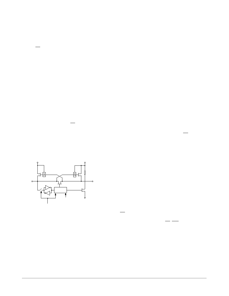
BIDIRECTIONAL LEVEL TRANSLATOR
This module (used on I/O/CRDIO, C4/CRDC4,
C8/CRDC8, Figure 24) adapts the signal voltage levels of
the I/O and control lines between the micro controller
(supplied by VBAT) and the smartcard (supplied by
CRDVCC)
When CS is low, with CRDVCC on, and start sequencing
completed, this module is transparent for the data, and acts
as if the card was directly connected to the reader
microcontroller. The core of the level shifter circuit defined
for the bidirectional CRDIO, CRDC4 and CRDC8 lines
consists of a NMOS switch which can be driven to the logic
low state from either side (microcontroller or card). If both
sides work in transmission mode with opposite phase, then
signal collision on the line is not avoidable. In this case, the
peak current is limited to a safe value for the integrated
circuit and the smartcard.
During hightolow transitions, the NMOS transistor
impedance (T1 = 250
W maximum) is low enough to charge
parasitic capacitance, and have a high enough dv/dt. On low
to high transition, the NMOS transistor is not active above
a certain voltage, and an acceleration circuit is activated to
ensure a high dv/dt.
When the chip is disabled (CS = H) with the voltage
supply CRDVCC still active, the I/O, C4 and C8 lines keep
their last logic state.
When the converter is off, a transistor forces the CRDIO,
CRDC4 and CRDC8 lines to a low state, thus preventing
any unwanted voltage level to be applied to the data lines
when the card is not in use.
Figure 24. Bidirectional Translator Functional Block
IO
VBAT
18 K
CONTROL
LOGIC
SEQ1 (SEQ3)
T2
CRDIO
CRDGND
CARDENABLE
(C4)
(C8)
T1
(CRDC4)
(CRDC8)
CRDVCC
SECURITY FEATURES
The MC33560 has a number of unique security functions
to guarantee that no electrical damage will be caused to the
smartcard:
Battery supply minimum voltage threshold
Card supply undervoltage and overcurrent detection
with automatic shutdown
Card pin overvoltage clamp to CRDVCC
Card presence detector for “clean” and fast shutdown
Consistent card signal sequencing at startup and
powerdown, according to ISO7816, even on error
conditions
Consistent clock signal, even when division ratio or
synchronization clock signal are changed “on the fly”
during a card session (Figure 29)
Active pulldown on all card pins, including CRDVCC,
when not in normal operating mode.
A current limiting function and an overtemperature
detector are limiting power dissipation.
ESD PROTECTION
Due to the nature of smartcards, the card interface pins
must absorb high Electro Static Discharge (ESD) energy
during card insertion. In addition, the control circuits
attached to these pins must safely withstand short circuits
and voltage transients during forced card extraction.
Therefore, the MC33560 features enhanced ESD
protection, current limitation and short circuit protection on
all smartcard interface pins, including C4 and C8.
PARALLEL OPERATION
For applications where two or more MC33560 are used,
the digital control and data bus lines are common to all
MC33560. Only the chip select signal, CS, requires a
separate line for each interface.
While deselected, all communication pins except
CRDCLK will keep their logical state on the card side, and
will go to high impedance mode on the microprocessor side.
Figure 31 shows a typical application of a dual card reader.
This arrangement was chosen only to illustrate the parallel
operation of two card interfaces in the same module. The
discrete capacitor components are necessary to provide low
impedance on the supply lines VBAT and CRDVCC and to
suppress the high frequency noise due to the DCDC
converter. The load resistors are external in order to adapt
the sense current of the “card present” switches.
MINIMUM POWER CONSUMPTION
CONSIDERATIONS
All analog blocks except the VBAT comparator and the
card presence detector are disabled in standby mode
(CS = H: DCDC converter stopped).
In order to maintain standby current at a minimum value,
all pins with pullup resistance (CS, INT, RDYMOD) have
to be kept in the high state or left open, and pins with
pulldown resistance (RESET, SYNCLK, PWRON) have
to be kept in the low state or left open. ASYCLKIN should
not be connected to an active clock signal during standby to
avoid dynamic currents. This is valid also for SYNCLK,
except that it can be left open.
相关PDF资料 |
PDF描述 |
|---|---|
| MC33689DDWBR2 | IC SYSTEM BASE W/LIN 32-SOIC |
| MC33742EPR2 | IC SYSTEM BASE W/CAN 48-QFN |
| MC33780EG | IC DBUS MASTER DUAL DIFF 16-SOIC |
| MC33790DW | IC DSI 2-CHAN INTERFACE 16-SOIC |
| MC33794EKR2 | IC SENSOR ELECTRIC FIELD 54SOICW |
相关代理商/技术参数 |
参数描述 |
|---|---|
| MC33560DWR2 | 功能描述:输入/输出控制器接口集成电路 3V/5V Smartcard RoHS:否 制造商:Silicon Labs 产品: 输入/输出端数量: 工作电源电压: 最大工作温度:+ 85 C 最小工作温度:- 40 C 安装风格:SMD/SMT 封装 / 箱体:QFN-64 封装:Tray |
| MC33560DWR2G | 功能描述:输入/输出控制器接口集成电路 3V/5V Smartcard Power Management RoHS:否 制造商:Silicon Labs 产品: 输入/输出端数量: 工作电源电压: 最大工作温度:+ 85 C 最小工作温度:- 40 C 安装风格:SMD/SMT 封装 / 箱体:QFN-64 封装:Tray |
| MC33565D | 功能描述:低压差稳压器 - LDO 3.3V 200mA w/Sleep RoHS:否 制造商:Texas Instruments 最大输入电压:36 V 输出电压:1.4 V to 20.5 V 回动电压(最大值):307 mV 输出电流:1 A 负载调节:0.3 % 输出端数量: 输出类型:Fixed 最大工作温度:+ 125 C 安装风格:SMD/SMT 封装 / 箱体:VQFN-20 |
| MC33565DG | 功能描述:低压差稳压器 - LDO 3.3V 200mA w/Sleep And Active Mode RoHS:否 制造商:Texas Instruments 最大输入电压:36 V 输出电压:1.4 V to 20.5 V 回动电压(最大值):307 mV 输出电流:1 A 负载调节:0.3 % 输出端数量: 输出类型:Fixed 最大工作温度:+ 125 C 安装风格:SMD/SMT 封装 / 箱体:VQFN-20 |
| MC33565DMR2 | 功能描述:低压差稳压器 - LDO 3.3V 200mA w/Sleep RoHS:否 制造商:Texas Instruments 最大输入电压:36 V 输出电压:1.4 V to 20.5 V 回动电压(最大值):307 mV 输出电流:1 A 负载调节:0.3 % 输出端数量: 输出类型:Fixed 最大工作温度:+ 125 C 安装风格:SMD/SMT 封装 / 箱体:VQFN-20 |
发布紧急采购,3分钟左右您将得到回复。