- 您现在的位置:买卖IC网 > PDF目录299472 > MC33689DWBR2 (Motorola, Inc.) System Basis Chip with LIN transceiver PDF资料下载
参数资料
| 型号: | MC33689DWBR2 |
| 厂商: | Motorola, Inc. |
| 英文描述: | System Basis Chip with LIN transceiver |
| 中文描述: | 系统基础芯片收发器和LIN |
| 文件页数: | 8/18页 |
| 文件大小: | 229K |
| 代理商: | MC33689DWBR2 |
MC33689
16
MC33689
6
SPI INTERFACE AND REGISTER DESCRIPTION
6.1
Data format description
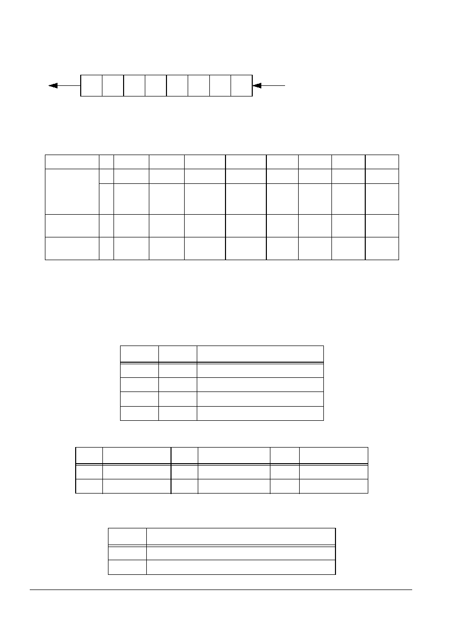
The SPI is an 8 bits SPI. All bits are data bytes. The MSB is send first. The minimum time between two rising edges on the
CSB pin is 15us.
During an SPI communication the state of MISO reports the state of the SBC, at time of CSB high to low transitions. The status
flag are latched at CSB high to low transitions.
Following tables describe the SPI register bit meaning, “reset value” and “bit reset condition”.
Note 1: The first SPI read, after reset, returns the BATFAIL flag state on bit D4.
D7 signals INT source. After INT occur, D7 read as a “1” means other bits report the INT source. D7 read as a “0” mean no INT
occurred and other bit report real time status.
6.2
Write control bits:
6.2.1
Mode control bits:
6.2.2
High side switches control bits:
6.2.3
LIN pull up termination control bits:
D7
D6
D5
D4
D3
D2
D1
D0
W
LINSL2
LINSL1
LIN-PU
HS3
HS2
HS1
Mode2
Mode1
R
INT
source
LINWU
or
LINFAIL
VSOV
VSUV
BATFAIL
(note1)
VddT
HSst
L2
L1
Write Reset
value
00
0
-
Write Reset
condition
POR,
RESET
POR,
RESET
POR
POR,
RESET
POR,
RESET
POR,
RESET
Mode 2
Mode 1
Description
0
Sleep mode
01
Stop mode
1
0
Normal mode + W/D clear
1
Normal mode
HS1
Description
HS2
Description
HS3
Description
0
HS1 off
0
HS2 off
0
HS3 off
1
HS1 on (if IN = 1)
1
HS2 on (if IN = 1)
1
HS3 on
LIN-PU
Description
0
30k pull up connected in sleep and stop mode
1
30k pull up disconnected in sleep and stop mode
MOSI
MISO
Bit0
Bit1
Bit2
Bit3
Bit4
Bit5
Bit6
Bit7
D0
D1
D2
D3
D4
D5
D6
D7
F
re
e
s
c
a
le
S
e
m
ic
o
n
d
u
c
to
r,
I
Freescale Semiconductor, Inc.
For More Information On This Product,
Go to: www.freescale.com
n
c
..
.
相关PDF资料 |
PDF描述 |
|---|---|
| MC33790DW/R2 | Two-Channel Distributed System Interface (DSI) Physical Interface Device |
| MC33794DH/R2 | Electric Field Imaging Device |
| MC33794DWB/R2 | Electric Field Imaging Device |
| MC33984PNA | Dual Intelligent High-Current Self-Protected Silicon High-Side Switch (4.0 mз) |
| MC56F8123 | 16-bit Hybrid Controllers |
相关代理商/技术参数 |
参数描述 |
|---|---|
| MC33690DWE | 功能描述:数字信号处理器和控制器 - DSP, DSC STAND ALONE TAG READER RoHS:否 制造商:Microchip Technology 核心:dsPIC 数据总线宽度:16 bit 程序存储器大小:16 KB 数据 RAM 大小:2 KB 最大时钟频率:40 MHz 可编程输入/输出端数量:35 定时器数量:3 设备每秒兆指令数:50 MIPs 工作电源电压:3.3 V 最大工作温度:+ 85 C 封装 / 箱体:TQFP-44 安装风格:SMD/SMT |
| MC33690DWER2 | 功能描述:数字信号处理器和控制器 - DSP, DSC STAND ALONE TAG READER RoHS:否 制造商:Microchip Technology 核心:dsPIC 数据总线宽度:16 bit 程序存储器大小:16 KB 数据 RAM 大小:2 KB 最大时钟频率:40 MHz 可编程输入/输出端数量:35 定时器数量:3 设备每秒兆指令数:50 MIPs 工作电源电压:3.3 V 最大工作温度:+ 85 C 封装 / 箱体:TQFP-44 安装风格:SMD/SMT |
| MC33696FCAE | 功能描述:射频收发器 UHF TRANSCEIVER RoHS:否 制造商:Atmel 频率范围:2322 MHz to 2527 MHz 最大数据速率:2000 Kbps 调制格式:OQPSK 输出功率:4 dBm 类型: 工作电源电压:1.8 V to 3.6 V 最大工作温度:+ 85 C 接口类型:SPI 封装 / 箱体:QFN-32 封装:Tray |
| MC33696FCAER2 | 功能描述:射频收发器 UHF TRANSCEIVER ECHO RoHS:否 制造商:Atmel 频率范围:2322 MHz to 2527 MHz 最大数据速率:2000 Kbps 调制格式:OQPSK 输出功率:4 dBm 类型: 工作电源电压:1.8 V to 3.6 V 最大工作温度:+ 85 C 接口类型:SPI 封装 / 箱体:QFN-32 封装:Tray |
| MC33696FCE | 功能描述:射频收发器 PLL Tuned UHF Recvr RoHS:否 制造商:Atmel 频率范围:2322 MHz to 2527 MHz 最大数据速率:2000 Kbps 调制格式:OQPSK 输出功率:4 dBm 类型: 工作电源电压:1.8 V to 3.6 V 最大工作温度:+ 85 C 接口类型:SPI 封装 / 箱体:QFN-32 封装:Tray |
发布紧急采购,3分钟左右您将得到回复。