- 您现在的位置:买卖IC网 > PDF目录359133 > MC33984 (飞思卡尔半导体(中国)有限公司) Dual Intelligent High-Current Self-Protected Silicon High-Side Switch (4.0 mOhm)(双智能大电流带自保护功能的硅高端开关(4mOhm)) PDF资料下载
参数资料
| 型号: | MC33984 |
| 厂商: | 飞思卡尔半导体(中国)有限公司 |
| 英文描述: | Dual Intelligent High-Current Self-Protected Silicon High-Side Switch (4.0 mOhm)(双智能大电流带自保护功能的硅高端开关(4mOhm)) |
| 中文描述: | 双智能大电流的自我保护硅高边开关(4.0毫欧)(双智能大电流带自保护功能的硅高端开关(4mOhm)) |
| 文件页数: | 17/24页 |
| 文件大小: | 783K |
| 代理商: | MC33984 |
MOTOROLA ANALOG INTEGRATED CIRCUIT DEVICE DATA
33984
17
Device Register Addressing
The following section describes the possible register
addresses and their impact on device operation.
Address x000—Status Register (STATR)
The START register is used to read the device status and the
various configuration register contents without disrupting the
device operation or the register contents. The register bits D2,
D1, D0 determine the content of the first eight bits of SO data.
When the register content is specific to one of the two outputs,
the bit D7 is used to select the desired output. In addition to the
device status, this feature provides the ability to read the
content of the OCR, SOCHLR, CDTOLR, DICR, OSDR, WDR
,
NAR, and UOVR registers. (Refer to the section entitled
Serial
Output Communication (Device Status Return Data)
beginning
on page 19.)
Address x001—Output Control Register (OCR)
The OCR register allows the MCU to control the outputs
through the SPI. Incoming message bit D0 reflects the desired
states of the high-side output HS0 (IN_SPI): a logic [1] enables
the output switch and a logic [0] turns it OFF. A logic [1] on
message bit D1 enables the Current Sense (CSNS) terminal.
Similarly, incoming message bit D2 reflects the desired states
of the high-side output HS1 (IN_SPI). A logic [1] enables the
output switch and a logic [0] turns it OFF. A logic [1] on
message bit D3 enables the CSNS terminal. In the event that
the current sense is enabled for both outputs, the current will be
summed. Bit D7 is used to feed the watchdog if enabled.
Address x010— Select Overcurrent High and Low Register
(SOCHLR)
The SOCHLR register allows the MCU to configure the
output overcurrent low and high detection levels, respectively.
Each output is independently selected for configuration based
on the state of the D7 bit; a write to this register when D7 is
logic [0] will configure the current detect levels for the HS0.
Similarly, if D7 is logic [1] when this register is written, HS1 is
configured. Each output can be configured to different levels. In
addition to protecting the device, this slow blow fuse emulation
feature can be used to optimize the load requirements matching
system characteristics. Bits D2–D0 set the overcurrent low
detection level to one of eight possible levels, as shown in
Table 3
. Bit D3 sets the overcurrent high detection level to one
of two levels, which is described in
Table 4
.
Address x011—Current Detection Time and Open Load
Register (CDTOLR)
The CDTOLR register is used by the MCU to determine the
amount of time the device will allow an overcurrent low
condition before output latches OFF occurs. Each output is
independently selected for configuration based on the state of
the D7 bit. A write to this register when bit 7 is logic [0] will
configure the timeout for the HS0. Similarly, if D7 is logic [1]
when this register is written, then HS1 is configured. Bits D1–
D0 allow the MCU to select one of four fault blanking times
defined in
Table 5
, page 18. Note that these timeouts apply only
to the overcurrent low detection levels. If the selected
overcurrent high level is reached, the device will latch off within
20
μ
s.
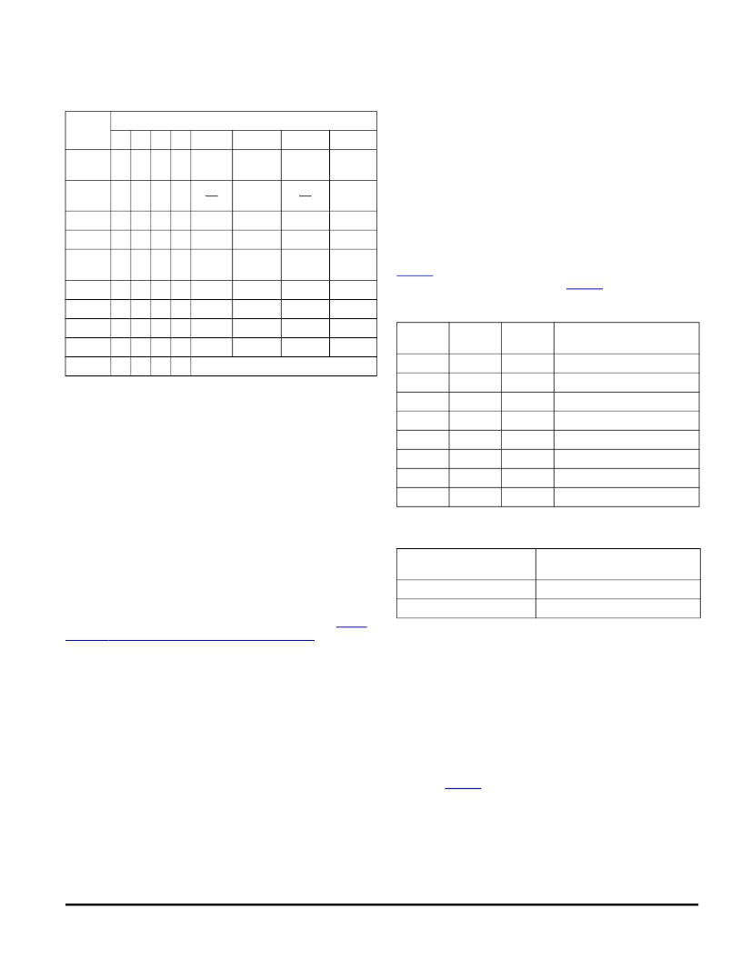
Table 2. Serial Input Address and Configuration Bit Map
SI
Register
Serial Input Data
D7 D6 D5 D4
D3
D2
D1
D0
STATR
SO
A3
0
0
0
0
SOA2
SOA1
SOA0
OCR
x
0
0
1
CSNS1
EN
IN1_SPI
CSNS0
EN
IN0_SPI
SOCHLR
s
0
1
0
SOCHs
SOCL2s
SOCL1s
SOCL0s
CDTOLR
s
0
1
1
OL DIS s CD DISs
OCLT1s
OCLT0s
DICR
s
1
0
0
FAST
SRs
CSNS
highs
IN DIS s
A/Os
OSDR
0
1
0
1
0
OSD2
OSD1
OSD0
WDR
1
1
0
1
0
0
WD1
WD0
NAR
0
1
1
0
0
0
0
0
UOVR
1
1
1
0
0
0
UV_dis
OV_dis
TEST
x
1
1
1
Motorola Internal Use (Test)
x = Don’t care.
s = Selection of output: logic [0] = HS0, logic [1] = HS1.
Table 3. Overcurrent Low Detection Levels
SOCL2
(D2)
SOCL1
(D1)
SOCL0
(D0)
Overcurrent Low Detection
(Amperes)
0
0
0
25
0
0
1
22.5
0
1
0
20
0
1
1
17.5
1
0
0
15
1
0
1
12.5
1
1
0
10
1
1
1
7.5
Table 4. Overcurrent High Detection Levels
SOCH (D3)
Overcurrent High Detection
(Amperes)
0
100
1
75
F
Freescale Semiconductor, Inc.
Go to: www.freescale.com
n
.
相关PDF资料 |
PDF描述 |
|---|---|
| MC33989 | System Basis Chip with High Speed CAN Transceiver(带高速CAN收发器的系统基片) |
| MC33990 | J-1850 SERIAL TRANSCEIVER(J-1850总线收发器) |
| MC33991 | Gauge Driver Integrated Circuit(标尺驱动器集成电路) |
| MC33993 | Multiple Switch Detection Interface(多开关监测接口) |
| MC33997 | Switching Power Supply with Linear Regulators(带线性稳压器的开关电源) |
相关代理商/技术参数 |
参数描述 |
|---|---|
| MC33984BPNA | 功能描述:电源开关 IC - 配电 SPD4 RoHS:否 制造商:Exar 输出端数量:1 开启电阻(最大值):85 mOhms 开启时间(最大值):400 us 关闭时间(最大值):20 us 工作电源电压:3.2 V to 6.5 V 电源电流(最大值): 最大工作温度:+ 85 C 安装风格:SMD/SMT 封装 / 箱体:SOT-23-5 |
| MC33984BPNAR2 | 功能描述:电源开关 IC - 配电 SPD4 RoHS:否 制造商:Exar 输出端数量:1 开启电阻(最大值):85 mOhms 开启时间(最大值):400 us 关闭时间(最大值):20 us 工作电源电压:3.2 V to 6.5 V 电源电流(最大值): 最大工作温度:+ 85 C 安装风格:SMD/SMT 封装 / 箱体:SOT-23-5 |
| MC33984CHFK | 功能描述:电源开关 IC - 配电 Dual 4mOhms smart RoHS:否 制造商:Exar 输出端数量:1 开启电阻(最大值):85 mOhms 开启时间(最大值):400 us 关闭时间(最大值):20 us 工作电源电压:3.2 V to 6.5 V 电源电流(最大值): 最大工作温度:+ 85 C 安装风格:SMD/SMT 封装 / 箱体:SOT-23-5 |
| MC33984CHFKR2 | 功能描述:电源开关 IC - 配电 Dual 4mOhms smart RoHS:否 制造商:Exar 输出端数量:1 开启电阻(最大值):85 mOhms 开启时间(最大值):400 us 关闭时间(最大值):20 us 工作电源电压:3.2 V to 6.5 V 电源电流(最大值): 最大工作温度:+ 85 C 安装风格:SMD/SMT 封装 / 箱体:SOT-23-5 |
| MC33984PNA | 制造商:Freescale Semiconductor 功能描述:POWER SWITCH HI SIDE 30A 16-PIN QFN - Trays |
发布紧急采购,3分钟左右您将得到回复。