- 您现在的位置:买卖IC网 > PDF目录371031 > MC34066P (MOTOROLA INC) Enhanced Product Single Voltage Detectors 5-SC70 -55 to 125 PDF资料下载
参数资料
| 型号: | MC34066P |
| 厂商: | MOTOROLA INC |
| 元件分类: | 稳压器 |
| 英文描述: | Enhanced Product Single Voltage Detectors 5-SC70 -55 to 125 |
| 中文描述: | 1.5 A SWITCHING CONTROLLER, 1000 kHz SWITCHING FREQ-MAX, PDIP16 |
| 封装: | PLASTIC, DIP-16 |
| 文件页数: | 7/12页 |
| 文件大小: | 168K |
| 代理商: | MC34066P |
MC34066 MC33066
7
MOTOROLA ANALOG IC DEVICE DATA
Errors in the threshold voltage and propagation delays
through the output drivers will affect the One–Shot period. To
guarantee accuracy, the output pulse of the control ship is
trimmed to within 5% of 1.5
μ
s with nominal values of RT
and CT.
The outputs of the Oscillator and One–Shot comparators
are OR’d together to produce the pulse ton, which drives the
Flip–Flop and output drivers. The output pulse ton is initiated
by the Oscillator, but either the oscillator comparator or the
One–Shot comparator can terminate the pulse. When the
oscillator discharge time exceeds the one–shot period, the
complete one–shot period is delivered to the output section. If
the oscillator discharge time is less than the one–shot period,
then the oscillator comparator terminates the pulse
prematurely and retriggers the One–Shot. The waveforms on
the left side of Figure 3 correspond to nonretriggered
operation with constant on–time and variable off–times. The
right side of Figure 3 represents retriggered operation with
variable on–time and constant off–time.
Error Amplifier
A fully accessible high performance Error Amplifier is
provided for feedback control of the power supply system.
The Error Amplifier is internally compensated and features dc
open loop gain greater than 70 dB, input offset voltage less
than 10 mV and guaranteed minimum gain–bandwidth
product of 2.5 MHz. The input common mode range extends
from 1.5 V to 5.1 V, which includes the reference voltage. For
common mode voltages below 1.5 V, the Error Amplifier
output is forced low providing minimum oscillator frequency.
The Oscillator Control Current pin is biased by the Error
Amplifier output voltage through RVFO as illustrated in Figure
4. The output swing of the Error Amplifier is restricted by a
clamp circuit to limit the maximum oscillator frequency. The
clamp circuit limits the voltage across RVFO to 2.5 V,
thus limiting IOSC to 2.5 V/RVFO. Oscillator accuracy is
improved by trimming the clamp voltage to obtain the
fOSC(high) specification of 1.0 MHz with nominal value
external components.
Osc Control
Current
3
IOSC
RVFO
Error Amp
Output
Error Amp
Noninverting Input
6
7
Error Amp
Inverting Input
8
Error Amp
Output Clamp
2.5V
EA Clamp
Error
Amplifier
–
+
–
+
Figure 4. Error Amplifier and Clamp
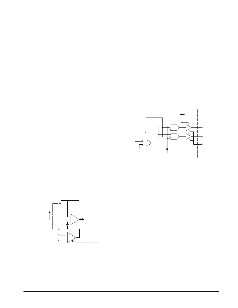
Output Section
The pulse, ton, generated by the Oscillator and One–Shot
timer is gated to dual totem pole output drives by the Steering
Flip–Flop shown in Figure 5. Positive transitions of ton toggle
the Flip–Flop, which causes the pulses to alternate between
Output A and Output B. The flip–flop is reset by the
undervoltage lockout circuit during startup to guarantee that
the first pulse appears at Output A.
The totem–pole output drives are ideally suited for driving
power MOSFETs and are capable of sourcing and sinking
1.5 A. Rise and fall times are typically 20 ns when driving a
1.0 nF load. High source/sink capability in a totem–pole
driver normally increases the risk of high cross conduction
current during output transitions. The MC34066 utilizes a
unique design that virtually eliminates cross conduction, thus
controlling the chip power dissipation at high frequencies. A
separate ground terminal is provided for the output drivers to
isolate the sensitive analog circuitry from large
transient currents.
Drivers
Steering
Flip–Flop
ton
T
Q
Q
R
14
12
13
Drive
Output A
Drive
Output B
Drive
Gnd
Fault
UVLO
VCC
Figure 5. Steering Flip–Flop and Output Drivers
PERIPHERAL SUPPORT FUNCTIONS
The MC34066 Resonant Controller provides a number of
support and protection functions including a precision voltage
reference, undervoltage lockout comparators, soft–start
circuitry, and a fault detector. These peripheral circuits ensure
that the power supply can be turned on and off in a safe,
controlled manner and that the system will be quickly
disabled when a fault condition occurs.
Undervoltage Lockout and Voltage Reference
Separate undervoltage lockout comparators sense the
input VCC voltage and the regulated reference voltage as
illustrated in Figure 6. When VCC increases to the upper
threshold voltage, the VCC UVLO comparator enables the
Reference Regulator. After the Vref output of the Reference
Regulator rises to 4.2 V, the Vref UVLO comparator switches
the UVLO signal to a logic zero state enabling the primary
control path. Reducing VCC to the lower threshold voltage
causes the VCC UVLO comparator to disable the Reference
Regulator. The Vref UVLO comparator then switches the
UVLO output to a logic one state disabling the controller.
相关PDF资料 |
PDF描述 |
|---|---|
| MC33066 | HIGH PERFORMANCE RESONANT MODE CONTROLLERS |
| MC34066 | HIGH PERFORMANCE RESONANT MODE CONTROLLERS |
| MC34080 | Low Quiescent Current, Programmable-Delay Supervisory Circuit 6-SOT-23 -40 to 125 |
| MC34081BD | Low Quiescent Current, Programmable-Delay Supervisory Circuit 6-SOT-23 -40 to 125 |
| MC34081BP | Low Quiescent Current, Programmable-Delay Supervisory Circuit 6-SON -40 to 125 |
相关代理商/技术参数 |
参数描述 |
|---|---|
| MC34067 | 制造商:ONSEMI 制造商全称:ON Semiconductor 功能描述:High Performance Resonant Mode Controllers |
| MC34067_05 | 制造商:ONSEMI 制造商全称:ON Semiconductor 功能描述:High Performance Resonant Mode Controllers |
| MC34067_09 | 制造商:ONSEMI 制造商全称:ON Semiconductor 功能描述:High Performance Resonant Mode Controllers |
| MC34067DW | 功能描述:DC/DC 开关控制器 High Performance RoHS:否 制造商:Texas Instruments 输入电压:6 V to 100 V 开关频率: 输出电压:1.215 V to 80 V 输出电流:3.5 A 输出端数量:1 最大工作温度:+ 125 C 安装风格: 封装 / 箱体:CPAK |
| MC34067DWG | 功能描述:DC/DC 开关控制器 High Performance Resonant Mode RoHS:否 制造商:Texas Instruments 输入电压:6 V to 100 V 开关频率: 输出电压:1.215 V to 80 V 输出电流:3.5 A 输出端数量:1 最大工作温度:+ 125 C 安装风格: 封装 / 箱体:CPAK |
发布紧急采购,3分钟左右您将得到回复。