- 您现在的位置:买卖IC网 > PDF目录22227 > MC34262PG (ON Semiconductor)IC PFC CONTROLLER CRM 8DIP PDF资料下载
参数资料
| 型号: | MC34262PG |
| 厂商: | ON Semiconductor |
| 文件页数: | 8/19页 |
| 文件大小: | 394K |
| 描述: | IC PFC CONTROLLER CRM 8DIP |
| 标准包装: | 50 |
| 模式: | 临界传导(CRM) |
| 电流 - 启动: | 250µA |
| 电源电压: | 12 V ~ 28 V |
| 工作温度: | 0°C ~ 85°C |
| 安装类型: | 通孔 |
| 封装/外壳: | 8-DIP(0.300",7.62mm) |
| 供应商设备封装: | 8-PDIP |
| 包装: | 管件 |
| 产品目录页面: | 1126 (CN2011-ZH PDF) |
| 其它名称: | MC34262PG-ND MC34262PGOS |
MC34262, MC33262
http://onsemi.com
8
A significant reduction in line current distortion can be
attained by forcing the preconverter to switch as the ac line
voltage crosses through zero. The forced switching is
achieved by adding a controlled amount of offset to the
Multiplier and Current Sense Comparator circuits. The
equation shown below accounts for the builtin offsets and
is accurate to within ten percent. Let V
th(M)
= 1.991 V
V
CS
, Pin 4 Threshold = 0.544 (V
Pin
2
V
th(M)
) V
Pin
3
+ 0.0417 (V
Pin
2
V
th(M)
)
Zero Current Detector
The MC34262 operates as a critical conduction current
mode controller, whereby output switch conduction is
initiated by the Zero Current Detector and terminated when
the peak inductor current reaches the threshold level
established by the Multiplier output. The Zero Current
Detector initiates the next ontime by setting the RS Latch
at the instant the inductor current reaches zero. This critical
conduction mode of operation has two significant benefits.
First, since the MOSFET cannot turnon until the inductor
current reaches zero, the output rectifier reverse recovery
time becomes less critical, allowing the use of an
inexpensive rectifier. Second, since there are no deadtime
gaps between cycles, the ac line current is continuous, thus
limiting the peak switch to twice the average input current.
The Zero Current Detector indirectly senses the inductor
current by monitoring when the auxiliary winding voltage
falls below 1.4 V. To prevent false tripping, 200 mV of
hysteresis is provided. Figure 10 shows that the thresholds
are welldefined over temperature. The Zero Current
Detector input is internally protected by two clamps. The
upper 6.7 V clamp prevents input overvoltage breakdown
while the lower 0.7 V clamp prevents substrate injection.
Current limit protection of the lower clamp transistor is
provided in the event that the input pin is accidentally
shorted to ground. The Zero Current Detector input to
Drive Output turnon propagation delay is typically 320 ns.
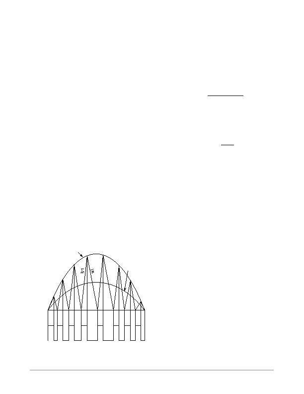
Figure 19. Inductor Current and MOSFET
Gate Voltage Waveforms
Inductor Current
Average
MOSFET
Q1
On
Off
0
Peak
Current Sense Comparator and RS Latch
The Current Sense Comparator RS Latch configuration
used ensures that only a single pulse appears at the Drive
Output during a given cycle. The inductor current is
converted to a voltage by inserting a groundreferenced
sense resistor R
7
in series with the source of output switch
Q1. This voltage is monitored by the Current Sense Input
and compared to a level derived from the Multiplier output.
The peak inductor current under normal operating
conditions is controlled by the threshold voltage of Pin 4
where:
Pin 4 Threshold
R
7
I
L(pk
) =
Abnormal operating conditions occur during
preconverter startup at extremely high line or if output
voltage sensing is lost. Under these conditions, the
Multiplier output and Current Sense threshold will be
internally clamped to 1.5 V. Therefore, the maximum peak
switch current is limited to:
1.5 V
R
7
I
pk(max)
=
An internal RC filter has been included to attenuate any
high frequency noise that may be present on the current
waveform. This filter helps reduce the ac line current
distortion especially near the zero crossings. With the
component values shown in Figure 21, the Current Sense
Comparator threshold, at the peak of the haversine varies
from 1.1 V at 90 Vac to 100 mV at 268 Vac. The Current
Sense Input to Drive Output turnoff propagation delay is
typically less than 200 ns.
Timer
A watchdog timer function was added to the IC to
eliminate the need for an external oscillator when used in
standalone applications. The Timer provides a means to
automatically start or restart the preconverter if the Drive
Output has been off for more than 620 ms after the inductor
current reaches zero. The restart time delay versus
temperature is shown in Figure 9.
Undervoltage Lockout and Quickstart
An Undervoltage Lockout comparator has been
incorporated to guarantee that the IC is fully functional
before enabling the output stage. The positive power
supply terminal (V
CC
) is monitored by the UVLO
comparator with the upper threshold set at 13 V and the
lower threshold at 8.0 V. In the standby mode, with V
CC
at 7.0 V, the required supply current is less than 0.4 mA.
This large hysteresis and low startup current allow the
implementation of efficient bootstrap startup techniques,
making these devices ideally suited for wide input range
offline preconverter applications. An internal 36 V
clamp has been added from V
CC
to ground to protect the IC
and capacitor C
4
from an overvoltage condition. This
feature is desirable if external circuitry is used to delay the
startup of the preconverter. The supply current, startup, and
operating voltage characteristics are shown in Figures 14
and 15.
相关PDF资料 |
PDF描述 |
|---|---|
| VE-J70-IZ | CONVERTER MOD DC/DC 5V 25W |
| SRR1260-391K | INDUCTOR POWER 390UH 1.08A SMD |
| R0.25D-153.3/H | CONV DC/DC 0.25W 15V +/-3.3VOUT |
| T95R226K050CZSL | CAP TANT 22UF 50V 10% 2824 |
| R0.25D-1524/P | CONV DC/DC 0.25W 15VIN +/-24VOUT |
相关代理商/技术参数 |
参数描述 |
|---|---|
| MC34262PG | 制造商:ON Semiconductor 功能描述:Power Supply IC |
| MC34268D | 功能描述:低压差稳压器 - LDO 2.85V 800mA SCSI-2 RoHS:否 制造商:Texas Instruments 最大输入电压:36 V 输出电压:1.4 V to 20.5 V 回动电压(最大值):307 mV 输出电流:1 A 负载调节:0.3 % 输出端数量: 输出类型:Fixed 最大工作温度:+ 125 C 安装风格:SMD/SMT 封装 / 箱体:VQFN-20 |
| MC34268DG | 功能描述:低压差稳压器 - LDO 2.85V 800mA SCSI-3 Active Terminator RoHS:否 制造商:Texas Instruments 最大输入电压:36 V 输出电压:1.4 V to 20.5 V 回动电压(最大值):307 mV 输出电流:1 A 负载调节:0.3 % 输出端数量: 输出类型:Fixed 最大工作温度:+ 125 C 安装风格:SMD/SMT 封装 / 箱体:VQFN-20 |
| MC34268DR2 | 功能描述:低压差稳压器 - LDO 2.85V 800mA SCSI-4 RoHS:否 制造商:Texas Instruments 最大输入电压:36 V 输出电压:1.4 V to 20.5 V 回动电压(最大值):307 mV 输出电流:1 A 负载调节:0.3 % 输出端数量: 输出类型:Fixed 最大工作温度:+ 125 C 安装风格:SMD/SMT 封装 / 箱体:VQFN-20 |
| MC34268DR2G | 功能描述:低压差稳压器 - LDO 2.85V 800mA SCSI-5 Active Terminator RoHS:否 制造商:Texas Instruments 最大输入电压:36 V 输出电压:1.4 V to 20.5 V 回动电压(最大值):307 mV 输出电流:1 A 负载调节:0.3 % 输出端数量: 输出类型:Fixed 最大工作温度:+ 125 C 安装风格:SMD/SMT 封装 / 箱体:VQFN-20 |
发布紧急采购,3分钟左右您将得到回复。