- 您现在的位置:买卖IC网 > PDF目录369901 > MC44826D (MOTOROLA INC) TV AND VCR I2C PLL TUNING CIRCUIT WITH 1.3 GHz PRESCALER AND MIX/OSC DECODER PDF资料下载
参数资料
| 型号: | MC44826D |
| 厂商: | MOTOROLA INC |
| 元件分类: | XO, clock |
| 英文描述: | TV AND VCR I2C PLL TUNING CIRCUIT WITH 1.3 GHz PRESCALER AND MIX/OSC DECODER |
| 中文描述: | PLL FREQUENCY SYNTHESIZER, 1300 MHz, PDSO14 |
| 封装: | PLASTIC, SO-14 |
| 文件页数: | 5/8页 |
| 文件大小: | 136K |
| 代理商: | MC44826D |
MC44826
5
MOTOROLA ANALOG IC DEVICE DATA
500 MHz
1.3 GHz
–j +j
0
2
0.5
1
0.5
1
2
0.5
1
2
ZO = 50
1.0 GHz
50 MHz
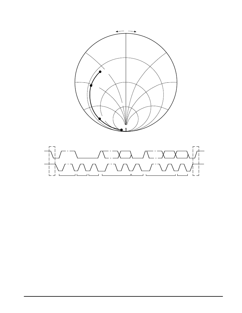
Figure 3. Typical HF Input Impedance
Figure 4. Complete Data Transfer Process
SDA
SCL
S
P
1–7
8
9
1–7
8
9
1–7
8
9
STA
ADDRESS
CA
R/W
ACK
DATA
ACK
DATA
ACK
STO
Data Format and Bus Receiver
The circuit receives the information for tuning and control
via the I2C bus. The incoming information, consisting of a
chip address byte followed by two or four data bytes, is
treated in the I2C bus receiver. The definition of the
permissible bus protocol is shown below:
1_STA
2_STA
3_STA
4_STA
CA
CA
CA
CA
CO
FM
CO
FM
BA
FL
BA
FL
STO
STO
FM
CO
FL
BA
STO
STO
STA = Start Condition
STO = Stop Condition
CA = Chip Address Byte
CO = Data Byte for Control Information
BA = Band Information
FM = Data Byte for Frequency Information (MSB’s)
FL = Data Byte for Frequency Information (LSB’s)
Figure 5 shows the five bytes of information that are
needed for circuit operation: there is the chip address, two
bytes of control and band information and two bytes of
frequency information.
After the chip address, two or four data bytes may be
received: if three data bytes are received the third data byte
is ignored.
If five or more data bytes are received the fifth and
following data bytes are ignored and the last acknowledge
pulse is sent at the end of the fourth data byte.
The first and the third data bytes contain a function bit
which allows the IC to distinguish between frequency
information and control plus band information.
Frequency information is preceded by a Logic “0”. If the
function bit is Logic “1” the two following bytes contain control
and band information. The first data byte, shifted after the
chip address, may be byte CO or byte FM.
The two permissible bus protocols with five bytes are
shown in Figure 5.
The Data and Clock inputs (Pins 10 and 11) are high
impedance when the supply voltage VCC1 is between 0 and
5.5 V.
相关PDF资料 |
PDF描述 |
|---|---|
| MC44827BDTB | LOW-POWER PLL TUNING CIRCUIT |
| MC44827 | LOW-POWER PLL TUNING CIRCUIT |
| MC44827DTB | LOW-POWER PLL TUNING CIRCUIT |
| MC44829D | TV AND VCR I2C PLL TUNING CIRCUIT WITH 1.3 GHz PRESCALER AND MIX/OSC DECODER |
| MC44829 | TV AND VCR I2C PLL TUNING CIRCUIT WITH 1.3 GHz PRESCALER AND MIX/OSC DECODER |
相关代理商/技术参数 |
参数描述 |
|---|---|
| MC44827 | 制造商:MOTOROLA 制造商全称:Motorola, Inc 功能描述:LOW-POWER PLL TUNING CIRCUIT |
| MC44827BDTB | 制造商:MOTOROLA 制造商全称:Motorola, Inc 功能描述:LOW-POWER PLL TUNING CIRCUIT |
| MC44827DTB | 制造商:Rochester Electronics LLC 功能描述:- Bulk 制造商:Motorola Inc 功能描述: |
| MC44829 | 制造商:MOTOROLA 制造商全称:Motorola, Inc 功能描述:TV AND VCR I2C PLL TUNING CIRCUIT WITH 1.3 GHz PRESCALER AND MIX/OSC DECODER |
| MC44829D | 制造商:MOTOROLA 制造商全称:Motorola, Inc 功能描述:TV AND VCR I2C PLL TUNING CIRCUIT WITH 1.3 GHz PRESCALER AND MIX/OSC DECODER |
发布紧急采购,3分钟左右您将得到回复。