- 您现在的位置:买卖IC网 > PDF目录26800 > MC54HC74AJ (ON SEMICONDUCTOR) HC/UH SERIES, DUAL POSITIVE EDGE TRIGGERED D FLIP-FLOP, COMPLEMENTARY OUTPUT, CDIP14 PDF资料下载
参数资料
| 型号: | MC54HC74AJ |
| 厂商: | ON SEMICONDUCTOR |
| 元件分类: | 锁存器 |
| 英文描述: | HC/UH SERIES, DUAL POSITIVE EDGE TRIGGERED D FLIP-FLOP, COMPLEMENTARY OUTPUT, CDIP14 |
| 封装: | CERAMIC, DIP-14 |
| 文件页数: | 3/7页 |
| 文件大小: | 229K |
| 代理商: | MC54HC74AJ |
MC54/74HC74A
High–Speed CMOS Logic Data
DL129 — Rev 6
3–3
MOTOROLA
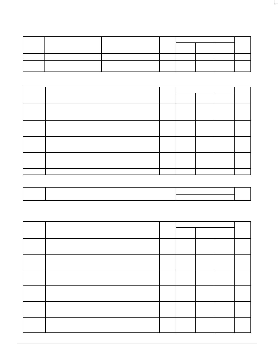
DC ELECTRICAL CHARACTERISTICS (Voltages Referenced to GND) – continued
Symbol
Parameter
Test Conditions
VCC
V
Guaranteed Limit
Unit
Symbol
Parameter
Test Conditions
VCC
V
– 55 to
25
_C
v 85_C
v 125_C
Unit
Iin
Maximum Input Leakage Current
Vin = VCC or GND
6.0
± 0.1
± 1.0
± 1.0
A
ICC
Maximum Quiescent Supply
Current (per Package)
Vin = VCC or GND
Iout = 0 A
6.0
2.0
20
80
A
NOTE: Information on typical parametric values can be found in Chapter 2 of the Motorola High–Speed CMOS Data Book (DL129/D).
AC ELECTRICAL CHARACTERISTICS (CL = 50 pF, Input tr = tf = 6.0 ns)
Symbol
Parameter
VCC
V
Guaranteed Limit
Unit
Symbol
Parameter
VCC
V
– 55 to
25
_C
v 85_C
v 125_C
Unit
fmax
Maximum Clock Frequency (50% Duty Cycle)
(Figures 1 and 4)
2.0
4.5
6.0
6.0
30
35
4.8
24
28
4.0
20
24
MHz
tPLH,
tPHL
Maximum Propagation Delay, Clock to Q or Q
(Figures 1 and 4)
2.0
4.5
6.0
100
20
17
125
25
21
150
30
26
ns
tPLH,
tPHL
Maximum Propagation Delay, Set or Reset to Q or Q
(Figures 2 and 4)
2.0
4.5
6.0
105
21
18
130
26
22
160
32
27
ns
tTLH,
tTHL
Maximum Output Transition Time, Any Output
(Figures 1 and 4)
2.0
4.5
6.0
75
15
13
95
19
16
110
22
19
ns
Cin
Maximum Input Capacitance
—
10
10
10
pF
NOTE: For propagation delays with loads other than 50 pF, and information on typical parametric values, see Chapter 2 of the Motorola High–
Speed CMOS Data Book (DL129/D).
CPD
Power Dissipation Capacitance (Per Flip–Flop)*
Typical @ 25
°C, VCC = 5.0 V
pF
CPD
Power Dissipation Capacitance (Per Flip–Flop)*
39
pF
* Used to determine the no–load dynamic power consumption: PD = CPD VCC2f + ICC VCC. For load considerations, see Chapter 2 of the
Motorola High–Speed CMOS Data Book (DL129/D).
TIMING REQUIREMENTS (Input tr = tf = 6.0 ns)
Symbol
Parameter
VCC
V
Guaranteed Limit
Unit
Symbol
Parameter
VCC
V
– 55 to
25
_C
v 85_C
v 125_C
Unit
tsu
Minimum Setup Time, Data to Clock
(Figure 3)
2.0
4.5
6.0
80
16
14
100
20
17
120
24
20
ns
th
Minimum Hold Time, Clock to Data
(Figure 3)
2.0
4.5
6.0
3.0
3.0
3.0
ns
trec
Minimum Recovery Time, Set or Reset Inactive to Clock
(Figure 2)
2.0
4.5
6.0
8.0
8.0
8.0
ns
tw
Minimum Pulse Width, Clock
(Figure 1)
2.0
4.5
6.0
60
12
10
75
15
13
90
18
15
ns
tw
Minimum Pulse Width, Set or Reset
(Figure 2)
2.0
4.5
6.0
60
12
10
75
15
13
90
18
15
ns
tr, tf
Maximum Input Rise and Fall Times
(Figures 1, 2, 3)
2.0
4.5
6.0
1000
500
400
1000
500
400
1000
500
400
ns
相关PDF资料 |
PDF描述 |
|---|---|
| MC54HCT157AJ | HCT SERIES, QUAD 2 LINE TO 1 LINE MULTIPLEXER, TRUE OUTPUT, CDIP16 |
| MC7400P | 74 SERIES, QUAD 2-INPUT NAND GATE, PDIP14 |
| MC7400L | 74 SERIES, QUAD 2-INPUT NAND GATE, CDIP14 |
| MC7401P | 74 SERIES, QUAD 2-INPUT NAND GATE, PDIP14 |
| MC741VHC157DR2 | AHC/VHC SERIES, QUAD 2 LINE TO 1 LINE MULTIPLEXER, TRUE OUTPUT, PDSO16 |
相关代理商/技术参数 |
参数描述 |
|---|---|
| MC54HC75J | 制造商:Motorola Inc 功能描述: |
| MC54HC86AJ | 制造商:MOTOROLA 制造商全称:Motorola, Inc 功能描述:Quad 2-Input Exclusive OR Gate |
| MC54HC86J | 制造商:MOTOROLA 制造商全称:Motorola, Inc 功能描述:Quad 2-Input Exclusive OR Gate |
| MC54HCT00A | 制造商:MOTOROLA 制造商全称:Motorola, Inc 功能描述:Quad 2-Input NAND Gate with LSTTL-Compatible Inputs |
| MC54HCT00AJ | 制造商:MOTOROLA 制造商全称:Motorola, Inc 功能描述:Quad 2-Input NAND Gate with LSTTL-Compatible Inputs |
发布紧急采购,3分钟左右您将得到回复。