- 您现在的位置:买卖IC网 > PDF目录1948 > MC56F8014MFAE (Freescale Semiconductor)IC DIGITAL SIGNAL CTLR 32-LQFP PDF资料下载
参数资料
| 型号: | MC56F8014MFAE |
| 厂商: | Freescale Semiconductor |
| 文件页数: | 93/124页 |
| 文件大小: | 0K |
| 描述: | IC DIGITAL SIGNAL CTLR 32-LQFP |
| 标准包装: | 1,250 |
| 系列: | 56F8xxx |
| 核心处理器: | 56800E |
| 芯体尺寸: | 16-位 |
| 速度: | 32MHz |
| 连通性: | I²C,SCI,SPI |
| 外围设备: | POR,PWM,WDT |
| 输入/输出数: | 26 |
| 程序存储器容量: | 16KB(8K x 16) |
| 程序存储器类型: | 闪存 |
| RAM 容量: | 2K x 16 |
| 电压 - 电源 (Vcc/Vdd): | 3 V ~ 3.6 V |
| 数据转换器: | A/D 8x12b |
| 振荡器型: | 内部 |
| 工作温度: | -40°C ~ 125°C |
| 封装/外壳: | 32-LQFP |
| 包装: | 托盘 |
第1页第2页第3页第4页第5页第6页第7页第8页第9页第10页第11页第12页第13页第14页第15页第16页第17页第18页第19页第20页第21页第22页第23页第24页第25页第26页第27页第28页第29页第30页第31页第32页第33页第34页第35页第36页第37页第38页第39页第40页第41页第42页第43页第44页第45页第46页第47页第48页第49页第50页第51页第52页第53页第54页第55页第56页第57页第58页第59页第60页第61页第62页第63页第64页第65页第66页第67页第68页第69页第70页第71页第72页第73页第74页第75页第76页第77页第78页第79页第80页第81页第82页第83页第84页第85页第86页第87页第88页第89页第90页第91页第92页当前第93页第94页第95页第96页第97页第98页第99页第100页第101页第102页第103页第104页第105页第106页第107页第108页第109页第110页第111页第112页第113页第114页第115页第116页第117页第118页第119页第120页第121页第122页第123页第124页
56F8014 Technical Data, Rev. 11
70
Freescale Semiconductor
The lower four bits of the GPIO A register can function as GPIO, PWM, or as additional clock output
signals. GPIO has priority and is enabled/disabled via the GPIOA_PEREN. If GPIOA[3:0] are
programmed to operate as peripheral outputs, then the choice between PWM and additional clock outputs
is done here in the CLKOUT. The default state is for the peripheral function of GPIOA[3:0] to be
programmed as PWM. This can be changed by altering PWM3 through PWM0.
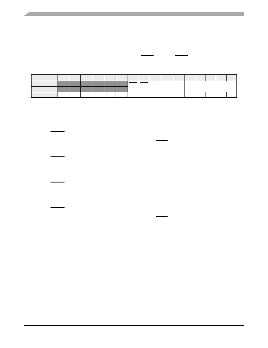
Figure 6-8 CLKO Select Register (SIM_CLKOUT)
6.3.7.1
Reserved—Bits 15–10
This bit field is reserved or not implemented. It is read as 0 and cannot be modified by writing.
6.3.7.2
PWM3—Bit 9
0 = Peripheral output function of GPIOA[3] is defined to be PWM3
1 = Peripheral output function of GPIOA[3] is defined to be the Relaxation Oscillator Clock
6.3.7.3
PWM2—Bit 8
0 = Peripheral output function of GPIOA[2] is defined to be PWM2
1 = Peripheral output function of GPIOA[2] is defined to be the system clock
6.3.7.4
PWM1—Bit 7
0 = Peripheral output function of GPIOA[1] is defined to be PWM1
1 = Peripheral output function of GPIOA[1] is defined to be two times the rate of the system clock
6.3.7.5
PWM0—Bit 6
0 = Peripheral output function of GPIOA[0] is defined to be PWM0
1 = Peripheral output function of GPIOA[0] is defined to be three times the rate of the system clock
6.3.7.6
Clockout Disable (CLKDIS)—Bit 5
0 = CLKOUT output is enabled and will output the signal indicated by CLKOSEL
1 = CLKOUT is 0
6.3.7.7
Clockout Select (CLKOSEL)—Bits 4–0
Selects clock to be muxed out on the CLKO pin.
00000 = Reserved for factory test—Continuous system clock
01001 = Reserved for factory test—OCCS MSTR OSC clock
01011 = Reserved for factory test—ADC clock
01100 = Reserved for factory test—JTAG TCLK
Base + $A
15
14
13
12
11
10
9
8
7
6
5
4
3
2
1
0
Read
0
PWM
3
PWM
2
PWM1PWM0
CLK
DIS
CLKOSEL
Write
RESET
0
000
0
1
0
相关PDF资料 |
PDF描述 |
|---|---|
| MC56F8023VLC | IC DSP 16BIT DUAL HARV 32-LQFP |
| MC56F8025VLD | IC DSP 16BIT DUAL HARV 44-LQFP |
| MC56F8036VLF | IC DGTL SGNL CTLR 16BIT 48-LQFP |
| MC56F8037VLH | IC DSP 16BIT DUAL 64-LQFP |
| MC56F8135VFGE | IC DIGITAL SIGNAL CTLR 128-LQFP |
相关代理商/技术参数 |
参数描述 |
|---|---|
| MC56F8014VFAE | 功能描述:数字信号处理器和控制器 - DSP, DSC 16 BIT DSPHC BAHAMAS RoHS:否 制造商:Microchip Technology 核心:dsPIC 数据总线宽度:16 bit 程序存储器大小:16 KB 数据 RAM 大小:2 KB 最大时钟频率:40 MHz 可编程输入/输出端数量:35 定时器数量:3 设备每秒兆指令数:50 MIPs 工作电源电压:3.3 V 最大工作温度:+ 85 C 封装 / 箱体:TQFP-44 安装风格:SMD/SMT |
| MC56F8023 | 制造商:FREESCALE 制造商全称:Freescale Semiconductor, Inc 功能描述:16-bit Digital Signal Controllers |
| MC56F8023VLC | 功能描述:数字信号处理器和控制器 - DSP, DSC 16 BIT DSPHC RoHS:否 制造商:Microchip Technology 核心:dsPIC 数据总线宽度:16 bit 程序存储器大小:16 KB 数据 RAM 大小:2 KB 最大时钟频率:40 MHz 可编程输入/输出端数量:35 定时器数量:3 设备每秒兆指令数:50 MIPs 工作电源电压:3.3 V 最大工作温度:+ 85 C 封装 / 箱体:TQFP-44 安装风格:SMD/SMT |
| MC56F8025 | 制造商:FREESCALE 制造商全称:Freescale Semiconductor, Inc 功能描述:16-bit Digital Signal Controllers |
| MC56F8025E | 制造商:FREESCALE 制造商全称:Freescale Semiconductor, Inc 功能描述:Digital Signal Controller Product Brief |
发布紧急采购,3分钟左右您将得到回复。